


MOTOROLA CMOS LOGIC DATA
6–215
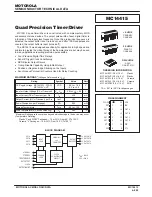
MC14490
TYPICAL APPLICATIONS
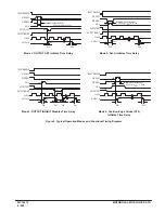
ASYMMETRICAL TIMING
In applications where different leading and trailing edge
delays are required (such as a fast attack/slow release
timer.) Clocks of different frequencies can be gated into the
MC14490 as shown in Figure 6. In order to produce a slow
attack/fast release circuit leads A and B should be inter-
changed. The clock out lead can then be used to feed clock
signals to the other MC14490 packages where the asym-
metrical input/output timing is required.
Figure 6. Fast Attack/Slow Release Circuit
IN
OUT
OSCout
MC14011B
OSCin
A
B
fC/N
EXTERNAL
CLOCK
÷
N
fC
MC14490
LATCHED OUTPUT
The contents of the Bounce Eliminator can be latched by
using several extra gates as shown in Figure 7. If the latch
lead is high the clock will be stopped when the output goes
low. This will hold the output low even though the input has
returned to the high state. Any time the clock is stopped the
outputs will be representative of the input signal four clock
periods earlier.
Figure 7. Latched Output Circuit
IN
OUT
OSCout
MC14011B
OSCin
MC14490
CLOCK
LATCH = 1
UNLATCH = 0
MULTIPLE TIMING SIGNALS
As shown in Figure 8, the Bounce Eliminator circuits can
be connected in series. In this configuration each output is
delayed by four clock periods relative to its respective input.
This configuration may be used to generate multiple timing
signals such as a delay line, for programming other timing
operations.
One application of the above is shown in Figure 9, where it
is required to have a single pulse output for a single opera-
tion (make) of the push button or relay contact. This only
requires the series connection of two Bounce Eliminator cir-
cuits, one inverter, and one NOR gate in order to generate
the signal AB as shown in Figures 9 and 10. The signal AB is
four clock periods in length. If the inverter is switched to the A
output, the pulse AB will be generated upon release or break
of the contact. With the use of a few additional parts many
different pulses and waveshapes may be generated.
Figure 8. Multiple Timing Circuit Connections
10
5
12
3
14
1
7
9
6
11
4
13
2
15
Aout
Bout
Cout
Dout
Eout
Fout
OSCin
CLOCK
B.E. 6
B.E. 5
B.E. 4
B.E. 3
B.E. 2
B.E. 1
OSCout
Ain
Bin
Cin
Din
Ein
Fin
Summary of Contents for CMOS Logic
Page 1: ......
Page 5: ...iv MOTOROLA CMOS LOGIC DATA ...
Page 6: ...Master Index 1 ...
Page 12: ...Product Selection Guide 2 ...
Page 17: ...The Better Program 3 ...
Page 20: ...B and UB Series Family Data 4 ...
Page 25: ...CMOS Handling and Design Guidelines 5 ...
Page 32: ...CMOS Handling and Design Guidelines 5 ...
Page 39: ...Data Sheets 6 ...
Page 234: ...MOTOROLA CMOS LOGIC DATA MC14174B 6 196 FUNCTIONAL BLOCK DIAGRAM TIMING DIAGRAM ...
Page 238: ...MOTOROLA CMOS LOGIC DATA MC14175B 6 200 FUNCTIONAL BLOCK DIAGRAM TIMING DIAGRAM ...
Page 555: ...CMOS Reliability 7 ...
Page 561: ...Equivalent Gate Count 8 ...
Page 563: ...Packaging Information Including Surface Mounts 9 ...
Page 571: ......