


MOTOROLA CMOS LOGIC DATA
6–77
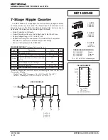
MC14027B
Dual J-K Flip-Flop
The MC14027B dual J–K flip–flop has independent J, K, Clock (C), Set (S)
and Reset (R) inputs for each flip–flop. These devices may be used in
control, register, or toggle functions.
•
Diode Protection on All Inputs
•
Supply Voltage Range = 3.0 Vdc to 18 Vdc
•
Logic Swing Independent of Fanout
•
Logic Edge–Clocked Flip–Flop Design —
Logic state is retained indefinitely with clock level either high or low;
information is transferred to the output only on the positive–going edge
of the clock pulse
•
Capable of Driving Two Low–power TTL Loads or One Low–power
Schottky TTL Load Over the Rated Temperature Range
•
Pin–for–Pin Replacement for CD4027B
ÎÎÎÎÎÎÎÎÎÎÎÎÎÎÎÎÎÎÎÎÎ
ÎÎÎÎÎÎÎÎÎÎÎÎÎÎÎÎÎÎÎÎÎ
MAXIMUM RATINGS*
(Voltages Referenced to VSS)
ÎÎÎÎ
ÎÎÎÎ
Symbol
ÎÎÎÎÎÎÎÎÎÎÎ
ÎÎÎÎÎÎÎÎÎÎÎ
Parameter
ÎÎÎÎÎÎ
ÎÎÎÎÎÎ
Value
ÎÎÎ
ÎÎÎ
Unit
ÎÎÎÎ
ÎÎÎÎ
VDD
ÎÎÎÎÎÎÎÎÎÎÎ
ÎÎÎÎÎÎÎÎÎÎÎ
DC Supply Voltage
ÎÎÎÎÎÎ
ÎÎÎÎÎÎ
– 0.5 to + 18.0
ÎÎÎ
ÎÎÎ
V
ÎÎÎÎ
ÎÎÎÎ
Vin, Vout
ÎÎÎÎÎÎÎÎÎÎÎ
ÎÎÎÎÎÎÎÎÎÎÎ
Input or Output Voltage (DC or Transient)
ÎÎÎÎÎÎ
ÎÎÎÎÎÎ
– 0.5 to VDD + 0.5
ÎÎÎ
ÎÎÎ
V
ÎÎÎÎ
Î
ÎÎ
Î
ÎÎÎÎ
lin, lout
ÎÎÎÎÎÎÎÎÎÎÎ
Î
ÎÎÎÎÎÎÎÎÎ
Î
ÎÎÎÎÎÎÎÎÎÎÎ
Input or Output Current (DC or Transient),
per Pin
ÎÎÎÎÎÎ
Î
ÎÎÎÎ
Î
ÎÎÎÎÎÎ
±
10
ÎÎÎ
Î
Î
Î
ÎÎÎ
mA
ÎÎÎÎ
ÎÎÎÎ
PD
ÎÎÎÎÎÎÎÎÎÎÎ
ÎÎÎÎÎÎÎÎÎÎÎ
Power Dissipation, per Package†
ÎÎÎÎÎÎ
ÎÎÎÎÎÎ
500
ÎÎÎ
ÎÎÎ
mW
ÎÎÎÎ
ÎÎÎÎ
Tstg
ÎÎÎÎÎÎÎÎÎÎÎ
ÎÎÎÎÎÎÎÎÎÎÎ
Storage Temperature
ÎÎÎÎÎÎ
ÎÎÎÎÎÎ
– 65 to + 150
ÎÎÎ
ÎÎÎ
_
C
ÎÎÎÎ
TL
ÎÎÎÎÎÎÎÎÎÎÎ
Lead Temperature (8–Second Soldering)
ÎÎÎÎÎÎ
260
ÎÎÎ
_
C
* Maximum Ratings are those values beyond which damage to the device may occur.
†Temperature Derating:
Plastic “P and D/DW” Packages: – 7.0 mW/
_
C From 65
_
C To 125
_
C
Ceramic “L” Packages: – 12 mW/
_
C From 100
_
C To 125
_
C
TRUTH TABLE
Inputs
Outputs*
C†
J
K
S
R
Qn‡
Qn+1
Qn+1
1
X
0
0
0
1
0
X
0
0
0
1
1
0
0
X
0
0
0
0
1
X
1
0
0
1
0
1
1
1
0
0
Qo
Qo
Qo
X
X
0
0
X
Qn
Qn
X
X
X
1
0
X
1
0
X
X
X
0
1
X
0
1
X
X
X
1
1
X
1
1
X = Don’t Care
‡ = Present State
† = Level Change
* = Next State
This device contains protection circuitry to guard against damage
due to high static voltages or electric fields. However, precautions must
be taken to avoid applications of any voltage higher than maximum rated
voltages to this high-impedance circuit. For proper operation, Vin and
Vout should be constrained to the range VSS
≤
(Vin or Vout)
≤
VDD.
Unused inputs must always be tied to an appropriate logic voltage
level (e.g., either VSS or VDD). Unused outputs must be left open.
No
Change
MOTOROLA
SEMICONDUCTOR TECHNICAL DATA
MC14027B
L SUFFIX
CERAMIC
CASE 620
ORDERING INFORMATION
MC14XXXBCP
Plastic
MC14XXXBCL
Ceramic
MC14XXXBD
SOIC
TA = – 55
°
to 125
°
C for all packages.
P SUFFIX
PLASTIC
CASE 648
D SUFFIX
SOIC
CASE 751B
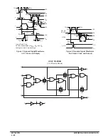
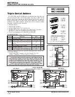
BLOCK DIAGRAM
12
11
13
10
9
4
5
3
6
7
14
15
2
1
S
S
R
R
K
C
J
K
C
J
Q
Q
Q
Q
VDD = PIN 16
VSS = PIN 8
Summary of Contents for CMOS Logic
Page 1: ......
Page 5: ...iv MOTOROLA CMOS LOGIC DATA ...
Page 6: ...Master Index 1 ...
Page 12: ...Product Selection Guide 2 ...
Page 17: ...The Better Program 3 ...
Page 20: ...B and UB Series Family Data 4 ...
Page 25: ...CMOS Handling and Design Guidelines 5 ...
Page 32: ...CMOS Handling and Design Guidelines 5 ...
Page 39: ...Data Sheets 6 ...
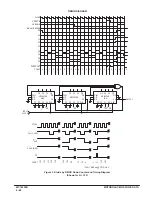
Page 234: ...MOTOROLA CMOS LOGIC DATA MC14174B 6 196 FUNCTIONAL BLOCK DIAGRAM TIMING DIAGRAM ...
Page 238: ...MOTOROLA CMOS LOGIC DATA MC14175B 6 200 FUNCTIONAL BLOCK DIAGRAM TIMING DIAGRAM ...
Page 555: ...CMOS Reliability 7 ...
Page 561: ...Equivalent Gate Count 8 ...
Page 563: ...Packaging Information Including Surface Mounts 9 ...
Page 571: ......