


MOTOROLA CMOS LOGIC DATA
6–501
MC14583B
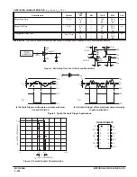
Figure 1. Typical Output Source and Sink Characteristics Test Circuit
NJ
VDD
Vout
VDD
VSS
SW1
SW2
VSS
IO
EXTERNAL
POWER
SUPPLY
Ain
DIS
Bin
Aout
Aout
Bout
Bout
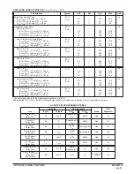
Output Source
Characteristics
Output Sink
Characteristics
Test
Value
VGS = – VDD
VDS = Vout – VDD
NJ
Test
Value
VGS = VDD
VDS = Vout
Output
Under Test
Switch Position
Switch Position
SW1
SW2
SW1
SW2
1
Aout, Bout
1
2
2
2
Aout, Bout
2
1
1
1
Exclusive OR
2
1
1
1
2
2
1
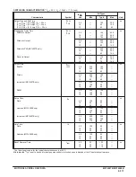
Figure 2. Power Dissipation Test Circuit and Waveforms
PULSE
GENERATOR 1
Ain
Aout
PULSE
GENERATOR 2
DIS
Bin
Aout
Bout
Bout
VDD
VSS
0.01
µ
F
CERAMIC
500
µ
F
CL
CL
CL
CL
CL
fout, Ain
fout, Bin
ID
Figure 3. Typical Threshold Points
POSITIVE
COMMON
NEGATIVE
R1
R2
POSITIVE
COMMON
NEGATIVE
R1
A — Feedback scheme for independent threshold adjustment:
B — Feedback scheme for hysteresis adjustment:
80
70
60
50
40
30
20
10
1.0 M
100 k
10 k
1.0 k
100
10 20 40
6 8
R1, R2, RESISTANCE (OHMS)
TYPICAL
THRESHOLD
POINT
(%V
DD
)
VDD = 5.0 V
VDD = 10 V
VDD = 15 V
VSS = 0
Summary of Contents for CMOS Logic
Page 1: ......
Page 5: ...iv MOTOROLA CMOS LOGIC DATA ...
Page 6: ...Master Index 1 ...
Page 12: ...Product Selection Guide 2 ...
Page 17: ...The Better Program 3 ...
Page 20: ...B and UB Series Family Data 4 ...
Page 25: ...CMOS Handling and Design Guidelines 5 ...
Page 32: ...CMOS Handling and Design Guidelines 5 ...
Page 39: ...Data Sheets 6 ...
Page 234: ...MOTOROLA CMOS LOGIC DATA MC14174B 6 196 FUNCTIONAL BLOCK DIAGRAM TIMING DIAGRAM ...
Page 238: ...MOTOROLA CMOS LOGIC DATA MC14175B 6 200 FUNCTIONAL BLOCK DIAGRAM TIMING DIAGRAM ...
Page 555: ...CMOS Reliability 7 ...
Page 561: ...Equivalent Gate Count 8 ...
Page 563: ...Packaging Information Including Surface Mounts 9 ...
Page 571: ......