


MOTOROLA CMOS LOGIC DATA
MC14528B
6–324
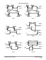
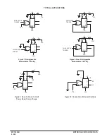
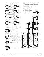
Figure 1. Output Source Current Test Circuit
Figure 2. Output Sink Current Test Circuit
VDD
VDD
OPEN
VSS
VSS
OPEN
VOL
RESET
A
B
Q
Q
16
8
16
8
IOL
RESET
A
B
Q
Q
IOH
VOH
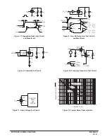
Figure 3. Power Dissipation Test Circuit and Waveforms
VDD
DUTY CYCLE = 50%
CL
CL
CL
CL
ID
500 pF
VSS
Vin
20 ns
20 ns
VDD
0 V
Vin
90%
10%
0.1
m
F
CERAMIC
RX
′
CX
′
RX
CX
A
B
RESET
A
′
B
′
RESET
′
Q
Q
Q
′
Q
′
ÎÎÎÎÎÎÎÎÎÎÎÎÎÎ
ÎÎÎÎÎÎÎÎÎÎÎÎÎÎ
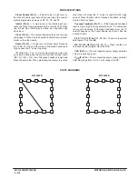
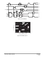
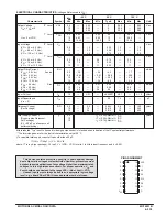
INPUT CONNECTIONS
Characteristics
Reset
A
B
tPLH, tPHL, tTLH, tTHL
tW
VDD
PG1
VDD
tPLH, tPHL, tTLH, tTHL
tW
VDD
VSS
PG2
tPLH(R), tPHL(R), tW
PG3
PG1
PG2
Figure 4. AC Test Circuit
PULSE
GENERATOR
PULSE
GENERATOR
PULSE
GENERATOR
VDD
RX
′
CX
′
RX
CX
VSS
A
B
RESET
A
′
B
′
RESET
′
Q
Q
Q
′
Q
′
CL
CL
CL
CL
PG1 =
PG2 =
PG3 =
*CX = 15 pF
*CL = 15 pF
RX = 5.0 k
W
* Includes capacitance of probes,
wiring, and fixture parasitic.
NOTE: AC test waveforms for
PG1, PG2, and PG3 on
next page.
Summary of Contents for CMOS Logic
Page 1: ......
Page 5: ...iv MOTOROLA CMOS LOGIC DATA ...
Page 6: ...Master Index 1 ...
Page 12: ...Product Selection Guide 2 ...
Page 17: ...The Better Program 3 ...
Page 20: ...B and UB Series Family Data 4 ...
Page 25: ...CMOS Handling and Design Guidelines 5 ...
Page 32: ...CMOS Handling and Design Guidelines 5 ...
Page 39: ...Data Sheets 6 ...
Page 234: ...MOTOROLA CMOS LOGIC DATA MC14174B 6 196 FUNCTIONAL BLOCK DIAGRAM TIMING DIAGRAM ...
Page 238: ...MOTOROLA CMOS LOGIC DATA MC14175B 6 200 FUNCTIONAL BLOCK DIAGRAM TIMING DIAGRAM ...
Page 555: ...CMOS Reliability 7 ...
Page 561: ...Equivalent Gate Count 8 ...
Page 563: ...Packaging Information Including Surface Mounts 9 ...
Page 571: ......