


MOTOROLA CMOS LOGIC DATA
6–267
MC14513B
ÎÎÎÎÎÎÎÎÎÎÎÎÎÎÎÎÎÎÎÎÎÎÎÎÎÎÎÎÎÎÎÎÎÎ
ÎÎÎÎÎÎÎÎÎÎÎÎÎÎÎÎÎÎÎÎÎÎÎÎÎÎÎÎÎÎÎÎÎÎ
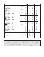
ELECTRICAL CHARACTERISTICS
(Voltages Referenced to VSS)
VDD
– 55
_
C
25
_
C
125
_
C
Characteristic
Symbol
VDD
Vdc
Min
Max
Min
Typ #
Max
Min
Max
Unit
Output Voltage — Segment Outputs
“0” Level
Vin = VDD or 0
VOL
5.0
10
15
—
—
—
0.05
0.05
0.05
—
—
—
0
0
0
0.05
0.05
0.05
—
—
—
0.05
0.05
0.05
Vdc
“1” Level
Vin = 0 or VDD
VOH
5.0
10
15
4.1
9.1
14.1
—
—
—
4.1
9.1
14.1
5.0
10
15
—
—
—
4.1
9.1
14.1
—
—
—
Vdc
Output Voltage — RBO Output
“0” Level
Vin = VDD or 0
VOL
5.0
10
15
—
—
—
0.05
0.05
0.05
—
—
—
0
0
0
0.05
0.05
0.05
—
—
—
0.05
0.05
0.05
Vdc
“1” Level
Vin = 0 or VDD
VOH
5.0
10
15
4.95
9.95
14.95
—
—
—
4.95
9.95
14.95
5.0
10
15
—
—
—
4.95
9.95
14.95
—
—
—
Vdc
Input Voltage #
“0” Level
(VO = 3.8 or 0.5 Vdc)
(VO = 8.8 or 1.0 Vdc)
(VO = 13.8 or 1.5 Vdc)
VIL
5.0
10
15
—
—
—
1.5
3.0
4.0
—
—
—
2.25
4.50
6.75
1.5
3.0
4.0
—
—
—
1.5
3.0
4.0
Vdc
(VO = 0.5 or 3.8 Vdc) “1” Level
(VO = 1.0 or 8.8 Vdc)
(VO = 1.5 or 13.8 Vdc)
VIH
5.0
10
15
3.5
7.0
11
—
—
—
3.5
7.0
11
2.75
5.50
8.25
—
—
—
3.5
7.0
11
—
—
—
Vdc
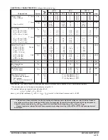
Output Drive Voltage — Segments
(IOH = 0 mA)
Source
(IOH = 5.0 mA)
(IOH = 10 mA)
(IOH = 15 mA)
(IOH = 20 mA)
(IOH = 25 mA)
VOH
5.0
4.1
—
3.9
—
3.4
—
—
—
—
—
—
—
4.1
—
3.9
—
3.4
—
4.57
4.24
4.12
3.94
3.70
3.54
—
—
—
—
—
—
4.1
—
3.5
—
3.0
—
—
—
—
—
—
—
Vdc
(IOH = 0 mA)
(IOH = 5.0 mA)
(IOH = 10 mA)
(IOH = 15 mA)
(IOH = 20 mA)
(IOH = 25 mA)
10
9.1
—
9.0
—
8.6
—
—
—
—
—
—
—
9.1
—
9.0
—
8.6
—
9.58
9.26
9.17
9.04
8.90
8.75
—
—
—
—
—
—
9.1
—
8.6
—
8.2
—
—
—
—
—
—
—
Vdc
(IOH = 0 mA)
(IOH = 5.0 mA)
(IOH = 10 mA)
(IOH = 15 mA)
(IOH = 20 mA)
(IOH = 25 mA)
15
14.1
—
14
—
13.6
—
—
—
—
—
—
—
14.1
—
14
—
13.6
—
14.59
14.27
14.18
14.07
13.95
13.80
—
—
—
—
—
—
14.1
—
13.6
—
13.2
—
—
—
—
—
—
—
Vdc
(continued)
This device contains protection circuitry to protect the inputs against damage due to high static voltages or electric fields; how-
ever, it is advised that normal precautions be taken to avoid application of any voltage higher than maximum rated voltages to this
high-impedance circuit. A destructive high current mode may occur if Vin and Vout is not constrained to the range VSS
≤
(Vin or
Vout)
≤
VDD.
Due to the sourcing capability of this circuit, damage can occur to the device if VDD is applied, and the outputs are shorted to
VSS and are at a logical 1 (See Maximum Ratings).
Unused inputs must always be tied to an appropriate logic voltage level (e.g., either VSS or VDD).
Summary of Contents for CMOS Logic
Page 1: ......
Page 5: ...iv MOTOROLA CMOS LOGIC DATA ...
Page 6: ...Master Index 1 ...
Page 12: ...Product Selection Guide 2 ...
Page 17: ...The Better Program 3 ...
Page 20: ...B and UB Series Family Data 4 ...
Page 25: ...CMOS Handling and Design Guidelines 5 ...
Page 32: ...CMOS Handling and Design Guidelines 5 ...
Page 39: ...Data Sheets 6 ...
Page 234: ...MOTOROLA CMOS LOGIC DATA MC14174B 6 196 FUNCTIONAL BLOCK DIAGRAM TIMING DIAGRAM ...
Page 238: ...MOTOROLA CMOS LOGIC DATA MC14175B 6 200 FUNCTIONAL BLOCK DIAGRAM TIMING DIAGRAM ...
Page 555: ...CMOS Reliability 7 ...
Page 561: ...Equivalent Gate Count 8 ...
Page 563: ...Packaging Information Including Surface Mounts 9 ...
Page 571: ......