


MOTOROLA CMOS LOGIC DATA
MC14517B
6–288
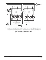
Dual 64-Bit Static Shift Register
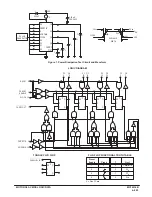
The MC14517B dual 64–bit static shift register consists of two identical,
independent, 64–bit registers. Each register has separate clock and write
enable inputs, as well as outputs at bits 16, 32, 48, and 64. Data at the data
input is entered by clocking, regardless of the state of the write enable input.
An output is disabled (open circuited) when the write enable input is high.
During this time, data appearing at the data input as well as the 16–bit,
32–bit, and 48–bit taps may be entered into the device by application of a
clock pulse. This feature permits the register to be loaded with 64 bits in 16
clock periods, and also permits bus logic to be used. This device is useful in
time delay circuits, temporary memory storage circuits, and other serial shift
register applications.
•
Diode Protection on All Inputs
•
Fully Static Operation
•
Output Transitions Occur on the Rising Edge of the Clock Pulse
•
Exceedingly Slow Input Transition Rates May Be Applied to the Clock
Input
•
3–State Output at 64th–Bit Allows Use in Bus Logic Applications
•
Shift Registers of any Length may be Fully Loaded with 16 Clock Pulses
•
Supply Voltage Range = 3.0 Vdc to 18 Vdc
•
Capable of Driving Two Low–power TTL Loads or One Low–power
Schottky TTL Load Over the Rated Temperature Range
ÎÎÎÎÎÎÎÎÎÎÎÎÎÎÎÎÎÎÎÎÎ
ÎÎÎÎÎÎÎÎÎÎÎÎÎÎÎÎÎÎÎÎÎ
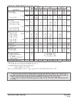
MAXIMUM RATINGS
(Voltages referenced to VSS)
ÎÎÎÎ
ÎÎÎÎ
Symbol
ÎÎÎÎÎÎÎÎÎÎÎ
ÎÎÎÎÎÎÎÎÎÎÎ
Parameter
ÎÎÎÎÎÎ
ÎÎÎÎÎÎ
Value
ÎÎÎ
ÎÎÎ
Unit
ÎÎÎÎ
VDD
ÎÎÎÎÎÎÎÎÎÎÎ
DC Supply Voltage
ÎÎÎÎÎÎ
– 0.5 to + 18.0
ÎÎÎ
V
ÎÎÎÎ
ÎÎÎÎ
Vin, Vout
ÎÎÎÎÎÎÎÎÎÎÎ
ÎÎÎÎÎÎÎÎÎÎÎ
Input or Output Voltage (DC or Transient)
ÎÎÎÎÎÎ
ÎÎÎÎÎÎ
– 0.5 to VDD + 0.5
ÎÎÎ
ÎÎÎ
V
ÎÎÎÎ
Î
ÎÎ
Î
ÎÎÎÎ
Iin, Iout
ÎÎÎÎÎÎÎÎÎÎÎ
Î
ÎÎÎÎÎÎÎÎÎ
Î
ÎÎÎÎÎÎÎÎÎÎÎ
Input or Output Current (DC or Transient),
per Pin
ÎÎÎÎÎÎ
Î
ÎÎÎÎ
Î
ÎÎÎÎÎÎ
±
10
ÎÎÎ
Î
Î
Î
ÎÎÎ
mA
ÎÎÎÎ
ÎÎÎÎ
PD
ÎÎÎÎÎÎÎÎÎÎÎ
ÎÎÎÎÎÎÎÎÎÎÎ
Power Dissipation, per Package†
ÎÎÎÎÎÎ
ÎÎÎÎÎÎ
500
ÎÎÎ
ÎÎÎ
mW
ÎÎÎÎ
ÎÎÎÎ
Tstg
ÎÎÎÎÎÎÎÎÎÎÎ
ÎÎÎÎÎÎÎÎÎÎÎ
Storage Temperature
ÎÎÎÎÎÎ
ÎÎÎÎÎÎ
– 65 to + 150
ÎÎÎ
ÎÎÎ
_
C
ÎÎÎÎ
ÎÎÎÎ
TL
ÎÎÎÎÎÎÎÎÎÎÎ
ÎÎÎÎÎÎÎÎÎÎÎ
Lead Temperature (8–Second Soldering)
ÎÎÎÎÎÎ
ÎÎÎÎÎÎ
260
ÎÎÎ
ÎÎÎ
_
C
* Maximum Ratings are those values beyond which damage to the device may occur.
†Temperature Derating:
Plastic “P and D/DW” Packages: – 7.0 mW/
_
C From 65
_
C To 125
_
C
Ceramic “L” Packages: – 12 mW/
_
C From 100
_
C To 125
_
C
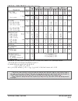
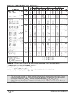
FUNCTIONAL TRUTH TABLE
(X = Don’t Care)
Clock
Write
Enable
Data
16–Bit Tap
32–Bit Tap
48–Bit Tap
64–Bit Tap
0
0
X
Content of 16–Bit
Displayed
Content of 32–Bit
Displayed
Content of 48–Bit
Displayed
Content of 64–Bit
Displayed
0
1
X
High Impedance
High Impedance
High Impedance
High Impedance
1
0
X
Content of 16–Bit
Displayed
Content of 32–Bit
Displayed
Content of 48–Bit
Displayed
Content of 64–Bit
Displayed
1
1
X
High Impedance
High Impedance
High Impedance
High Impedance
0
Data entered
into 1st Bit
Content of 16–Bit
Displayed
Content of 32–Bit
Displayed
Content of 48–Bit
Displayed
Content of 64–Bit
Displayed
1
Data entered
into 1st Bit
Data at tap
entered into 17–Bit
Data at tap
entered into 33–Bit
Data at tap
entered into 49–Bit
High Impedance
0
X
Content of 16–Bit
Displayed
Content of 32–Bit
Displayed
Content of 48–Bit
Displayed
Content of 64–Bit
Displayed
1
X
High Impedance
High Impedance
High Impedance
High Impedance
MOTOROLA
SEMICONDUCTOR TECHNICAL DATA
MC14517B
L SUFFIX
CERAMIC
CASE 620
ORDERING INFORMATION
MC14XXXBCP
Plastic
MC14XXXBCL
Ceramic
MC14XXXBDW
SOIC
TA = – 55
°
to 125
°
C for all packages.
P SUFFIX
PLASTIC
CASE 648
DW SUFFIX
SOIC
CASE 751G
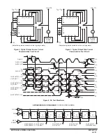
PIN ASSIGNMENT
13
14
15
16
9
10
11
12
5
4
3
2
1
8
7
6
CB
WEB
Q48B
Q16B
VDD
DB
Q32B
Q64B
CA
WEA
Q48A
Q16A
VSS
Q32A
Q64A
DA
Summary of Contents for CMOS Logic
Page 1: ......
Page 5: ...iv MOTOROLA CMOS LOGIC DATA ...
Page 6: ...Master Index 1 ...
Page 12: ...Product Selection Guide 2 ...
Page 17: ...The Better Program 3 ...
Page 20: ...B and UB Series Family Data 4 ...
Page 25: ...CMOS Handling and Design Guidelines 5 ...
Page 32: ...CMOS Handling and Design Guidelines 5 ...
Page 39: ...Data Sheets 6 ...
Page 234: ...MOTOROLA CMOS LOGIC DATA MC14174B 6 196 FUNCTIONAL BLOCK DIAGRAM TIMING DIAGRAM ...
Page 238: ...MOTOROLA CMOS LOGIC DATA MC14175B 6 200 FUNCTIONAL BLOCK DIAGRAM TIMING DIAGRAM ...
Page 555: ...CMOS Reliability 7 ...
Page 561: ...Equivalent Gate Count 8 ...
Page 563: ...Packaging Information Including Surface Mounts 9 ...
Page 571: ......