


DLQ-3000+
Rev. A
2-20
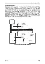
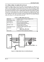
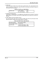
2.3.3 Memory Back-up Circuit
When the printer power is turned off, mainly the following data is backed up in the
EEPROM AT93C66 (IC23).
Paper length, TOF, TEAR OFF, left and right margins, line spacing, pitch
selection, character code, character fonts, high speed print, print direction,
customer code
Interface setting
Values used for controlling the mechanism (condition for all the sensors)
Adjusted values used for controlling the mechanism (i.e. Bi-D adjustment, PG
adjustment and PG
α
value)
IPD ID for the boot strap program
The first operation date, accumulated print amount, accumulated power-on time
and timing for ribbon replacement
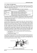
Data to be backed up is transferred by the gate array as serial data. At printer power off, the
gate array outputs the chip select signal ESC from port 126 and data to be backed-up is
sent to the EEPROM from port 124 (EDO) before the power supply voltage completely
drops. The data stored in the EEPROM is read by sending data to the EDI terminal in the
gate array when the printer is turned on. ECK is the clock signal for synchronization.
C S
D I
D O
E E P R O M
A T 9 3 C 6 6
S K
E C K
E C S
E D I
E D O
E 0 5 B 4 6
G a t e A r r a y
Figure 2-14.Memory Back-up Circuit Block Diagram
Summary of Contents for DLQ-3000 Minerva+
Page 1: ...EPSON 24 PIN DOT MATRIX PRINTER EPSON DLQ 3000 SERVICE MANUAL SEIKO EPSON CORPORATION 4008259 ...
Page 5: ...v REVISION SHEET Revision Issued Data Contents Rev A August 21 1997 First Release ...
Page 61: ...2 3 12 Other Sensor Circuits 2 31 ...
Page 160: ...Chapter 6 Maintenance 6 1 Maintenance 6 1 6 1 1 Lubrication and Adhesion 6 1 ...
Page 171: ...DLQ 3000 Rev A A 6 ...
Page 172: ...Appendix Rev A A 7 A 2 Circuit Diagrams Figure A 2 C210 MAIN Board Circuit Diagram 1 2 ...
Page 173: ...DLQ 3000 Rev A A 8 ...
Page 174: ...Appendix Rev A A 9 Figure A 3 C210 MAIN Board Circuit Diagram 2 2 ...
Page 175: ...DLQ 3000 Rev A A 10 ...
Page 177: ...DLQ 3000 Rev A A 12 Figure A 5 C124 PSB Board Circuit Diagram ...
Page 180: ...Appendix Rev A A 15 Figure A 8 C210 MAIN Board Component Layout 2 2 ...
Page 181: ...DLQ 3000 Rev A A 16 Figure A 9 C124 PSB Board Component Layout ...
Page 182: ...Appendix Rev A A 17 Figure A 10 C124 PSE Board Component Layout ...
Page 189: ...EPSON SEIKO EPSON CORPORATION ...