


DLQ-3000+
Rev. A
2-14
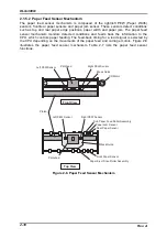
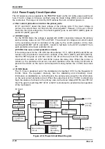
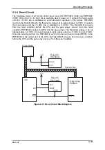
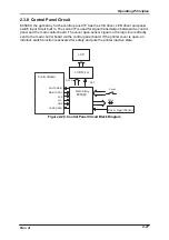
2.2.2 Power Supply Circuit Operation
The AC power source is supplied to the PSB/PSE board via the AC cable, power switch and
fuse. The AC voltage is full-wave rectified using the diode bridge (DB1) and smoothed by
the condenser. The surge cut circuit by SCR reduces the rush current at power-on.
Over current protection circuit on the primary side
IC101 and IC201 detect the input voltage of the primary side. If the input voltage is
normal, the current does not flow into the shunt-regulator. However, if the over current
flows into the input voltage line, the shunt-regulator goes on and Q103 (Q203) goes on
and Q101 (Q201) goes off.
+35 VDC block
For the 35VDC block, the voltage is applied with AC/DC conversion between the primary
and secondary sides via coil T101 and T201. The amount of voltage and current output
to the secondary circuit is controlled at the gate by the on/off operation of the main
switching MOS FET (Q101 and Q201). Control is fed back to the Q101 and Q201 from
each protection circuit and controller circuit.
[+35 VDC line over current protection circuit]
If the voltage level for the +35 VDC line drops below +13 V, Q153 (Q253) and Q154 are
turned on by the detector circuit which consists of the R173 (R273) and R174 (R274),
then the PC102 goes on and the current cuts off as the result. At this time, the delay
circuit which consists of C157 and R154 makes the delay time. When the printer is
turned on, the protection circuit can not start operation since the delay circuit acts to
prevent the drivers on the main control board from rising before the +5 VDC lines rises
up.
+5 VDC block
The +5 V line is produced out of the stabilized and sm35 V by the Regulator IC
TL494. Since the regulator internally has the stabilizing and smoothing circuit,
information on stabilization is not fed back to the primary side except for the information
on the over current protection circuit. When the output level of the +5 VDC is abnormally
high, the status is fed back to the primary side via the Zener diode (ZD153) and PC102,
then The gate for switching FET Q101 or Q201 is shortened to avoid abnormal operation
of the mechanism.
AC Power
Fuse
EMI Filter
Diode Bridge
Surge Cut
Smoothing
Circuit
Main Switching
Circuit
Half-wave
Rectifier
Smoothing
Circuit
PC101
PC102
PC 201
Regulator IC
Constant Voltage
Circuit
Protection Circuit
+5 VDC
+35 VDC
(CH. B)
+35 VDC
(CH. A)
Main Switching
Circuit
Half-wave
Rectifier
Smoothing
Circuit
Figure 2-10. Power Circuit Block Diagram
Summary of Contents for DLQ-3000 Minerva+
Page 1: ...EPSON 24 PIN DOT MATRIX PRINTER EPSON DLQ 3000 SERVICE MANUAL SEIKO EPSON CORPORATION 4008259 ...
Page 5: ...v REVISION SHEET Revision Issued Data Contents Rev A August 21 1997 First Release ...
Page 61: ...2 3 12 Other Sensor Circuits 2 31 ...
Page 160: ...Chapter 6 Maintenance 6 1 Maintenance 6 1 6 1 1 Lubrication and Adhesion 6 1 ...
Page 171: ...DLQ 3000 Rev A A 6 ...
Page 172: ...Appendix Rev A A 7 A 2 Circuit Diagrams Figure A 2 C210 MAIN Board Circuit Diagram 1 2 ...
Page 173: ...DLQ 3000 Rev A A 8 ...
Page 174: ...Appendix Rev A A 9 Figure A 3 C210 MAIN Board Circuit Diagram 2 2 ...
Page 175: ...DLQ 3000 Rev A A 10 ...
Page 177: ...DLQ 3000 Rev A A 12 Figure A 5 C124 PSB Board Circuit Diagram ...
Page 180: ...Appendix Rev A A 15 Figure A 8 C210 MAIN Board Component Layout 2 2 ...
Page 181: ...DLQ 3000 Rev A A 16 Figure A 9 C124 PSB Board Component Layout ...
Page 182: ...Appendix Rev A A 17 Figure A 10 C124 PSE Board Component Layout ...
Page 189: ...EPSON SEIKO EPSON CORPORATION ...