


Product Description
Rev. A
1-29
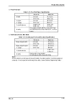
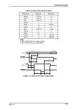
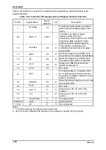
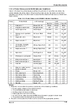
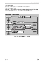
Table 1-24. Data Transmission Timing
Parameter
Minimum
Maximum
tsetup
500 ns
thold
500 ns
tstb
500 ns
tready
0
tbusy
500 ns
treply
tack
500 ns
10
µ
s
tnbusy
0
tnext
0
tt-out *
1
120 ns
tt-in *
2
200 ns
Note:
1. Rise and fall time for output signals
2. Rise and fall time for input signal
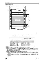
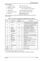
S T O R B E
D A T A ( n )
D A T A
D A T A ( n + 1 )
A C K N L G
B U S Y
t h o l d
t s e t u p
t s t b
t r e a d y t b u s y
t r e p l y
t a c k
t n b u s y
t n e x t
Figure 1-14. Data Transmission Timing Chart
Summary of Contents for DLQ-3000 Minerva+
Page 1: ...EPSON 24 PIN DOT MATRIX PRINTER EPSON DLQ 3000 SERVICE MANUAL SEIKO EPSON CORPORATION 4008259 ...
Page 5: ...v REVISION SHEET Revision Issued Data Contents Rev A August 21 1997 First Release ...
Page 61: ...2 3 12 Other Sensor Circuits 2 31 ...
Page 160: ...Chapter 6 Maintenance 6 1 Maintenance 6 1 6 1 1 Lubrication and Adhesion 6 1 ...
Page 171: ...DLQ 3000 Rev A A 6 ...
Page 172: ...Appendix Rev A A 7 A 2 Circuit Diagrams Figure A 2 C210 MAIN Board Circuit Diagram 1 2 ...
Page 173: ...DLQ 3000 Rev A A 8 ...
Page 174: ...Appendix Rev A A 9 Figure A 3 C210 MAIN Board Circuit Diagram 2 2 ...
Page 175: ...DLQ 3000 Rev A A 10 ...
Page 177: ...DLQ 3000 Rev A A 12 Figure A 5 C124 PSB Board Circuit Diagram ...
Page 180: ...Appendix Rev A A 15 Figure A 8 C210 MAIN Board Component Layout 2 2 ...
Page 181: ...DLQ 3000 Rev A A 16 Figure A 9 C124 PSB Board Component Layout ...
Page 182: ...Appendix Rev A A 17 Figure A 10 C124 PSE Board Component Layout ...
Page 189: ...EPSON SEIKO EPSON CORPORATION ...