


Product Description
Rev. A
1-23
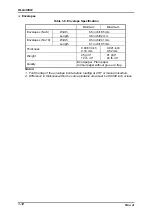
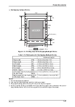
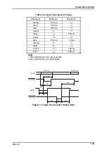
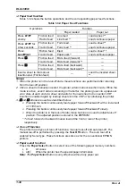
Overlapping multi-part forms with labels
P W
T M
R M B
B M
P L
L M B
L M
R M
L a b e l
R O L
B O L
T O L
L O L
L a b e l
P r i n t a b l e A r e a
P r i n t a b l e A r e a
P e r f o r a t i o n
: P r i n t a b l e A r e a
T M
L F L
T F L
B F L
R F L
Figure 1-13. Printable Area for Overlapping Multi-Part Forms with Labels
Table 1-20. Printable Area for Overlapping Multi-Part Forms
Continuous paper
Paper width
(PW)
Refer to Section 1.3.4.
Paper length
(PL)
Refer to Section 1.3.4.
Left margin
(LM)
19 mm (0.748”) or more
Right margin
(RM)
19 mm (0.748”) or more
Left margin from the multi-part forms
to the base sheet
(LMB)
13 mm (0.552”) ± 3 mm (0.118”)
Right margin from the multi-part forms
to the base sheet
(RMB)
13 mm (0.552”) ± 3 mm (0.118”)
Top margin
(TM)
21.2 mm (0.835”) or more
Bottom margin
(BM)
4.2 mm (0.165”) or more
Non-printable area
(NA)
25.4 mm (1.0”) or more
Left margin from label
(LFL)
45 mm (1.77”) or more
Right margin from label
(RFL)
45 mm (1.77”) or more
Top margin from label
(TFL)
25 mm(0.984”) or more
Bottom margin from label
(BFL)
25 mm(0.984”) or more
Left margin on label
(LOL)
3 mm (0.118”) or more
Right margin on label
(ROL)
3 mm (0.118”) or more
Top margin on label
(TOL)
3 mm (0.118”) or more
Bottom margin on label
(BOL)
3 mm (0.118”) or more
Notes:
1. Do not feed paper backward.
2. The paper feeding pitch in the top 75 mm (2.9”) may be irregular.
Summary of Contents for DLQ-3000 Minerva+
Page 1: ...EPSON 24 PIN DOT MATRIX PRINTER EPSON DLQ 3000 SERVICE MANUAL SEIKO EPSON CORPORATION 4008259 ...
Page 5: ...v REVISION SHEET Revision Issued Data Contents Rev A August 21 1997 First Release ...
Page 61: ...2 3 12 Other Sensor Circuits 2 31 ...
Page 160: ...Chapter 6 Maintenance 6 1 Maintenance 6 1 6 1 1 Lubrication and Adhesion 6 1 ...
Page 171: ...DLQ 3000 Rev A A 6 ...
Page 172: ...Appendix Rev A A 7 A 2 Circuit Diagrams Figure A 2 C210 MAIN Board Circuit Diagram 1 2 ...
Page 173: ...DLQ 3000 Rev A A 8 ...
Page 174: ...Appendix Rev A A 9 Figure A 3 C210 MAIN Board Circuit Diagram 2 2 ...
Page 175: ...DLQ 3000 Rev A A 10 ...
Page 177: ...DLQ 3000 Rev A A 12 Figure A 5 C124 PSB Board Circuit Diagram ...
Page 180: ...Appendix Rev A A 15 Figure A 8 C210 MAIN Board Component Layout 2 2 ...
Page 181: ...DLQ 3000 Rev A A 16 Figure A 9 C124 PSB Board Component Layout ...
Page 182: ...Appendix Rev A A 17 Figure A 10 C124 PSE Board Component Layout ...
Page 189: ...EPSON SEIKO EPSON CORPORATION ...