


Section 13 Serial Communication Interface (SCI)
Rev.2.00 Jun. 28, 2007 Page 514 of 666
REJ09B0311-0200
13.7.7 Serial
Data
Reception (Except in Block Transfer Mode)
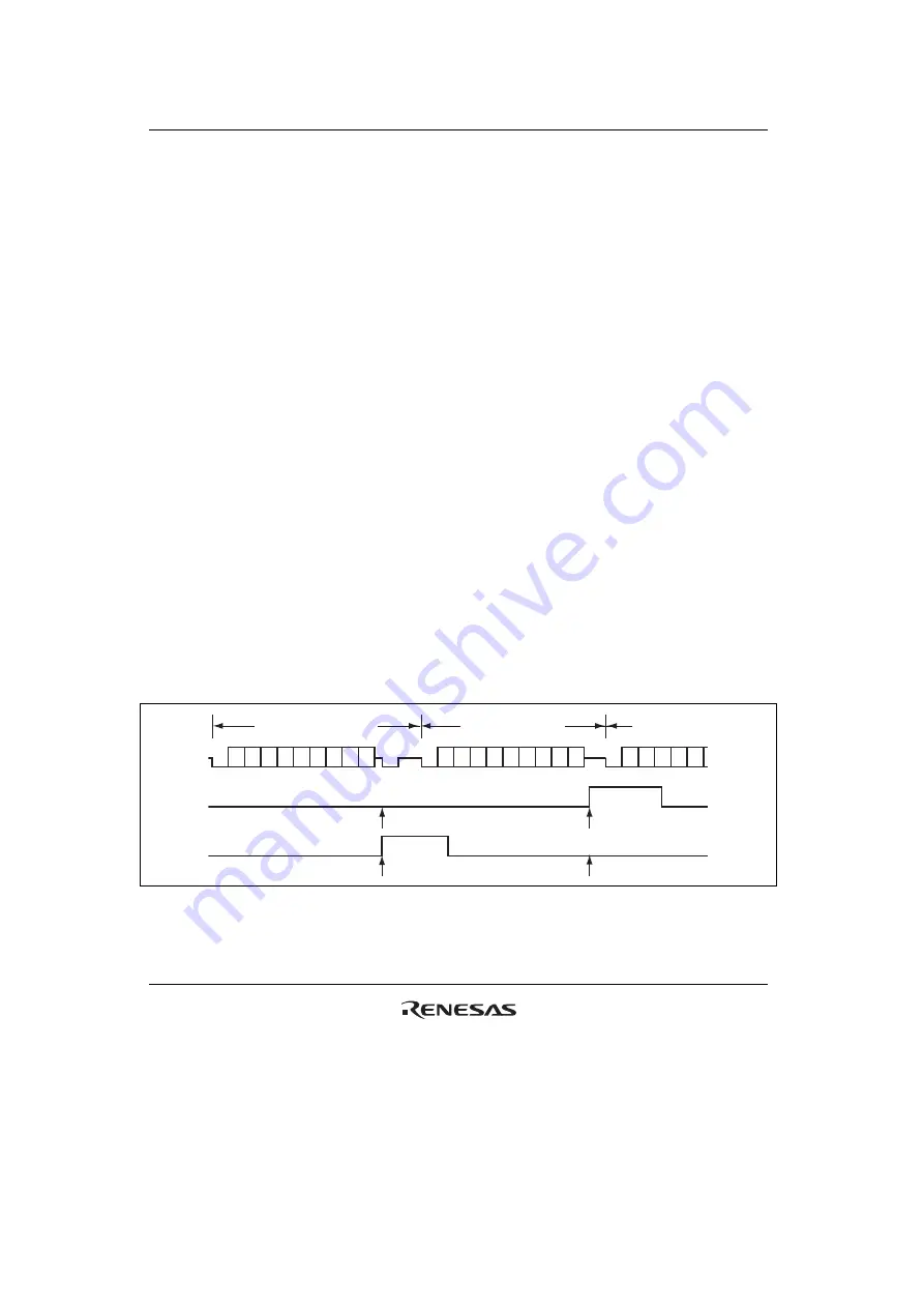
Data reception in smart card interface mode is similar to that in normal serial communication
interface mode. Figure 13.29 shows the data re-transfer operation during reception.
1. If a parity error is detected in receive data, the PER bit in SSR is set to 1. Here, an ERI
interrupt request is generated if the RIE bit in SCR is set to 1. Clear the PER bit to 0 before the
next parity bit is sampled.
2. For the frame in which a parity error is detected, the RDRF bit in SSR is not set to 1.
3. If no parity error is detected, the PER bit in SSR is not set to 1.
4. In this case, data is determined to have been received successfully, and the RDRF bit in SSR is
set to 1. Here, an RXI interrupt request is generated if the RIE bit in SCR is set to 1.
Figure 13.30 shows a sample flowchart for reception. All the processing steps are automatically
performed using an RXI interrupt request to activate the DTC. In reception, setting the RIE bit to 1
allows an RXI interrupt request to be generated when the RDRF flag is set to 1. This activates the
DTC by an RXI request thus allowing transfer of receive data if the RXI interrupt request is
specified as a source of DTC activation beforehand. The RDRF flag is automatically cleared to 0
at data transfer by the DTC. If an error occurs during reception, i.e., either the ORER or PER flag
is set to 1, a transmit/receive error interrupt (ERI) request is generated and the error flag must be
cleared. If an error occurs, the DTC is not activated and receive data is skipped, therefore, the
number of bytes of receive data specified in the DTC is transferred. Even if a parity error occurs
and the PER bit is set to 1 in reception, receive data is transferred to RDR, thus allowing the data
to be read.
Note: For operations in block transfer mode, see section 13.4, Operation in Asynchronous Mode.
D0 D1 D2 D3 D4 D5 D6 D7 Dp DE
Ds D0 D1 D2 D3 D4 D5 D6 D7 Dp
(DE)
Ds D0 D1 D2 D3 D4
Ds
(n + 1) th
transfer frame
Retransfer frame
nth transfer frame
RDRF
[1]
PER
[2]
[3]
[4]
Figure 13.29 Data Re-Transfer Operation in SCI Reception Mode
Содержание H8SX/1650
Страница 2: ...Rev 2 00 Jun 28 2007 Page ii of xxii...
Страница 106: ...Section 4 Exception Handling Rev 2 00 Jun 28 2007 Page 84 of 666 REJ09B0311 0200...
Страница 142: ...Section 5 Interrupt Controller Rev 2 00 Jun 28 2007 Page 120 of 666 REJ09B0311 0200...
Страница 326: ...Section 8 I O Ports Rev 2 00 Jun 28 2007 Page 304 of 666 REJ09B0311 0200...
Страница 470: ...Section 12 Watchdog Timer WDT Rev 2 00 Jun 28 2007 Page 448 of 666 REJ09B0311 0200...
Страница 546: ...Section 13 Serial Communication Interface SCI Rev 2 00 Jun 28 2007 Page 524 of 666 REJ09B0311 0200...
Страница 566: ...Section 14 A D Converter Rev 2 00 Jun 28 2007 Page 544 of 666 REJ09B0311 0200...
Страница 574: ...Section 16 RAM Rev 2 00 Jun 28 2007 Page 552 of 666 REJ09B0311 0200...
Страница 584: ...Section 17 Clock Pulse Generator Rev 2 00 Jun 28 2007 Page 562 of 666 REJ09B0311 0200...
Страница 638: ...Section 19 List of Registers Rev 2 00 Jun 28 2007 Page 616 of 666 REJ09B0311 0200...
Страница 668: ...Section 20 Electrical Characteristics Rev 2 00 Jun 28 2007 Page 646 of 666 REJ09B0311 0200...
Страница 676: ...Appendix Rev 2 00 Jun 28 2007 Page 654 of 666 REJ09B0311 0200...
Страница 688: ...Rev 2 00 Jun 28 2007 Page 666 of 666 REJ09B0311 0200...
Страница 691: ......
Страница 692: ...H8SX 1650 Group Hardware Manual...


