background image

Rev. 3.0, 03/01, page 329 of 390

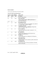
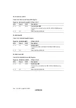
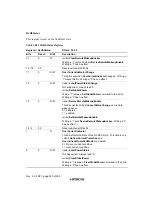
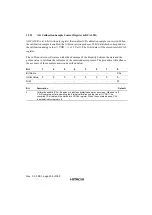
HcRhDescriptorB

This register is only rest by a power-on reset (PCIRST#). It is written during system initialization
to configure the Root Hub. These bit should not be written during normal operation.

Table 18.42 HcRhDescriptorB Register

Register:  HcRhDescriptorB

Offset:  4C-4F

Bits

Reset

R/W

Description

31 - 16

0000h

R/W

PortPowerControlMask

USB Host Controller implements global-power switching.  This
field is only valid if NoPowerSwitching is cleared and
PowerSwitchingMode is set (individual port switching).  When
set, the port only responds to individual port power switching
commands (Set/ClearPortPower).  When cleared, the port only
responds to global power switching commands
(Set/ClearGlobalPower).
0 = Global power switching
1 = Individual port switching

Port Bit relationship
16 : Reserved
17 : Port 1
18 : Port 2
...
31 : Port 15

Unimplemented ports are reserved, read/write '0'.

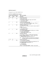
15 - 0

0000h

R/W

DeviceRemoveable

USB Host Controller ports default to removable devices.
0 = Device removable
1 = Device not removable

Port Bit relationship
0 : Reserved
1 : Port 1
2 : Port 2
...
15 : Port 15

Unimplemented ports are reserved, read/write '0'.

Содержание HD64465

Страница 1: ...Windows CE Intelligent Peripheral Controller HD64465 User s Manual ADE 602 168B Rev 3 0 03 08 01 Hitachi Ltd ...

Страница 2: ...of bodily injury such as aerospace aeronautics nuclear power combustion control transportation traffic safety equipment or medical equipment for life support 4 Design your application so that the product is used within the ranges guaranteed by Hitachi particularly for maximum rating operating supply voltage range heat radiation characteristics installation conditions and other characteristics Hita...

Страница 3: ...l Names by pin numbers in alphabetical order 26 Table 4 4 Pin Descriptions of CPU Interface Signal name of R1 pin Former Edition RESET This Edition RESETPI Table 4 24 Pin Descriptions of No Connected Pins Correct the table name Former Edition Pin Descriptions of LCD Interface This Edition Pin Descriptions of No Connected Pins 39 Table 4 25 Pin Descriptions of Power Ground Pin description of AVSS3 ...

Страница 4: ... the description ofACCLK pin 71 7 3 1 Port Data Register Former Edition GPCDR Address 100004018h This Edition GPEDR Address H 100004018 91 Table 9 1 The Register List of Timer Module Former Edition Register Size 2 Access Size 2 This Edition Register Size 16 Access Size 16 93 9 2 3 TRVR1 Timer 1 Read Vlue Register 94 9 2 4 TRVR0 Timer 0 Read Value Register Former Edition R W value R O This Edition ...

Страница 5: ...ion Unit µs ns 336 19 2 1 A D Data Registers A to D ADDRA to ADDRD ADCAL Former Edition Bit 9 AD8 Bit 8 AD9 This Edition Bit 9 AD9 Bit 8 AD8 341 19 3 2 Acan Mode SCAN 1 Add the ADCSR table 352 353 Table 20 13 AFECK clock input AC Timing Spec PLL1 bypass unit ns Table 20 14 AFECK clock input AC Timing Spec PLL1 operatings unit ns Table 20 15 AFECK clock input AC Timing Spec PLL2 bypass unit ns Tabl...

Страница 6: ...used No problem no standby time added Certain interval allowed between PLL standby and wakeup Several seconds may be required for access by HD64465BP from CPU 3 Countermeasures Use the system in a state without any problem by referring to 2 above Create your program in a way to prohibit access other than to the HD64465BP system configuration register offset address H 00000000 to H 00000ff0 for a c...

Страница 7: ...er 4 1 15 10 bit ADC 4 1 16 Package 4 Section 2 General Description 5 Section 3 System Block Diagram 7 3 1 Application Circuit 7 3 2 System Block Diagram 8 3 3 Physical Address Space 9 3 4 HD64465 Memory Address 10 3 5 Pin Configuration 11 3 5 1 HD64465BP Top View 11 3 5 2 HD64465BP Bottom View 12 3 5 3 HD64465BQ Top View 13 3 5 4 HD64465BQ Bottom View 14 Section 4 Pin Description 15 Section 5 Int...

Страница 8: ... Register SPLLCR 63 6 3 7 System Revision Register SRR 64 6 3 8 System Device ID Register SDID 64 6 4 System Hardware Reset Timing 65 6 4 1 Power On Reset Output 65 6 4 2 Manual Reset Output 66 Section 7 General Purpose I O Port 67 7 1 Overview 67 7 1 1 Features 67 7 2 Register Configuration 69 7 3 Register Descriptions 70 7 3 1 Port Data Register 70 7 3 2 Port Control Register 72 7 3 3 Port Inter...

Страница 9: ...9 2 12 PWM0CS PWM 0 Clock Scale Register 102 9 2 13 PWM0LPC PWM 0 Low Pulse Width Counter Register 103 9 2 14 PWM0HPC PWM 0 High Pulse Width Counter Register 104 9 3 Special Register Programming Sequence 104 9 4 Interrupt Timing 104 9 5 A D Trigger Signal ADTRIG 106 9 6 DMA Request Enable Function 108 9 7 PWM Operation 108 Section 10 PC Card Controller PCC 109 10 1 Overview 109 10 2 Features 109 1...

Страница 10: ...IR 156 Section 12 UART 157 12 1 Overview 157 12 2 Features 157 12 3 Serial Channel Register Description 158 12 3 1 Data Register 158 12 3 2 Control Registers UIER UIIR UFCR UDLL UDLM ULCR UMCR 159 12 3 3 Status Register ULSR and UMSR 164 12 4 Reset 167 12 5 Programming 168 12 5 1 Programming Sequence 168 12 6 Software Reset 168 12 7 Clock Input Operation 168 12 8 FIFO Interrupt Mode Operation 169 ...

Страница 11: ...OCS 201 14 2 18 AC97 Transmit Interrupt Enable Register ATIER 202 14 2 19 AC97 TX FIFO Status Register 205 14 2 20 AC97 RX FIFO Interrupt Enable Register ARIER 208 14 2 21 AC97 RX Status Register ARSR 211 14 2 22 AC97 Control Register ACR 213 14 2 23 AC97 TAG Register ATAGR 215 14 2 24 Slot Request Active Register SRAR 216 14 3 Function Description 217 14 3 1 Internal Bus Interface 217 14 3 2 Cloc...

Страница 12: ...agram 244 16 2 Register Description 245 16 2 1 Control Register CR 245 16 2 2 Status Register SR 246 16 2 3 H8 Control 1 Register H8C1R 247 16 2 4 H8 Control 2 Register H8C2R 247 16 3 Function Description 247 16 4 Timing Diagram 247 Section 17 PS 2 Interface 249 17 1 Overview 249 17 2 Pin Configuration 249 17 3 Registers Description 249 17 3 1 Keyboard Control Status Register KBCSR 250 17 3 2 Keyb...

Страница 13: ...D ADCAL 336 19 2 2 A D Control Status Register ADCSR 337 19 2 3 A D Calibration Sample Control Register ADCALCR 338 19 3 Operation 339 19 3 1 Single Mode SCAN 0 339 19 3 2 Scan Mode SCAN 1 341 19 3 3 Input Sampling and A D Conversion Time 343 19 3 4 A D External Trigger Input Timing 344 19 4 Interrupts 344 19 5 Usage Notes 345 19 6 A D Conversion Characteristics 345 19 7 Analog Input Pin Character...

Страница 14: ...e 37 Table 4 20 Pin Descriptions of PS 2 Interface 38 Table 4 21 Pin Descriptions of System Reset Interface 38 Table 4 22 Pin Descriptions of Crystal Interface 38 Table 4 23 Pin Description of Miscellaneous Interface 38 Table 4 24 Pin Descriptions of LCD Interface 39 Table 4 25 Pin Descriptions of Power Ground 39 Table 6 1 The Register List of Power Management and System Configuration 52 Table 7 1...

Страница 15: ...R and Host Controller Action 275 Table 18 2 ITD Packet Offset Location 276 Table 18 3 Completion Codes 279 Table 18 4 Dword0 GTD Fields 282 Table 18 5 Dword0 ITD Fields 282 Table 18 6 Dword1 GTD Fields 282 Table 18 7 Dword1 ITD Fields 283 Table 18 8 Dword2 Fields 283 Table 18 9 Dword3 GTD Fields 283 Table 18 10 Dword3 ITD Fields 283 Table 18 11 Offset0 Field Description 284 Table 18 12 List Proces...

Страница 16: ... 4 A D Conversion Time Single Mode 344 Table 19 5 A D Conversion Characteristics 345 Table 19 6 Analog Input Pin Characteristics 346 Table 20 1 DC Electrical Characteristics Ta 0 C to 70 C 347 Table 20 2 CPU Interface AC Timing Spec 349 Table 20 3 Crystal Oscillator and PLL Settle AC Timing Spec 349 Table 20 4 GPIO AC Timing Spec 349 Table 20 5 I O Port Interrupt AC Timing Spec 350 Table 20 6 PCMC...

Страница 17: ...IO 8 106 Figure 9 5 Interrupt Request Timer1 0r Timing Diagram in Case Prescale 1 16 Timer1 0_clk CKIO 16 106 Figure 9 6 A D Trigger Signal ADTRIG Timing Diagram in Case Prescale 1 Timer0_clk CKIO 107 Figure 9 7 A D Trigger Signal ADTRIG Timing Diagram in Case Prescale 1 4 Timer0_clk CKIO 4 107 Figure 9 8 A D Trigger Signal ADTRIG Timing Diagram in Case Prescale 1 8 Timer0_clk CKIO 8 107 Figure 9 ...

Страница 18: ... Data Packet Format 297 Figure 18 11 Handshake Packet Format 297 Figure 18 12 Preamble Packet Format 298 Figure 18 13 Serializer 299 Figure 18 14 CRC Logic 300 Figure 18 15 Non Isochronous Bus Transaction 304 Figure 18 16 Isochronous Bus Transaction 305 Figure 19 1 A D Converter Block Diagram 334 Figure 19 2 Example of A D Converter Operation Single Mode Channel 1 Selected 340 Figure 19 3 Example ...

Страница 19: ...ming 360 Figure 20 18 SCDI DMA Request Timing 361 Figure 20 19 Cold Reset Timing 361 Figure 20 20 Warm Reset Timing 361 Figure 20 21 SCDI Sync and Data Timing 362 Figure 20 22 AFE Interface Access Timing 362 Figure 20 23 Keyboard Controller Interface Read Timing 363 Figure 20 24 Keyboard Controller Interface Write Timing 363 Figure 20 25 USB Over Current Detect to Power Down Timing 363 Figure 20 2...

Страница 20: ...3V or 5V operation is fully supported for PCMCIA address data and control signals Supports TI TPS2206 serial interface Supports STANDBY mode 1 3 AFE Interface Supports SGS THOMSON STLC7546 and STLC7550 interface Read buffer and write buffer are provided for performance enhancement Supports STANDBY mode 1 4 GPIO Function Port Interrupt GPIO pins can be programmed as input output ports or as interru...

Страница 21: ...reloaded timer with pre scale 1 1 4 1 8 1 16 for dividing CKIO Supports generating DMA or Interrupt request whenever timer s count reaches zero Supports generating ADC external trigger whenever timer s count reaches zero Provides two channel Pulse Width Modulation PWM for VR control of LCD Supports STANDBY mode 1 8 Keyboard Controller Interface Supports ISA bus like interface to pair with the exte...

Страница 22: ...be supported by PIO or DMA mode access The Codec Interface is able to provide SM3 Slave Mode for communication with CS4218 and CS4271 and SM3 Master Mode for CS4218 Supports AC97 version 1 03 and version 2 0 serial link interface Supports STANDBY mode 1 12 IrDA Supports HP SIR or ASKIR infrared interface Supports FIR and MIR Provides DMA channel mode for FIR Supports STANDBY mode 1 13 Clock Genera...

Страница 23: ...d for USB Open Host Controller driver to store frame lists transaction descriptors for USB host controller s schedule control and this local memory is also used as data buffer for host controller to send receive data to from USB devices 1 15 10 bit ADC 10 bit resolution Provides four input channels High speed conversion conversion time is maximum 10 µs per channel Two conversion modes Single mode ...

Страница 24: ...el port interface controller keyboard interface CS4218 CS4271 AC97 Codec interface IrDA controller USB Host controller AC97 Codec 10 bit ADC and power management unit This chip pairs with SH 4 SH7709 SH3 DSP processors and features all the key peripheral functions required by the sub sub notebooks designed for Windows CE v2 0 and above providing a total solution for Windows CE Mini NoteBook Subsub...

Страница 25: ...Rev 3 0 03 01 page 6 of 390 ...

Страница 26: ...3 System Block Diagram 3 1 Application Circuit ROM Keyboard Controller IrDA MIC STLC7546 DAA 32 SH 4 SH7709 32 32 HD64465 CS4218 CS4271 AC97 UART PRINTER 8 KEYBOARD SPEAKER TOUCH PAD DRAM USB Devices 32 PCMCIA 0 Touch Panel PS 2 Keyboard ...

Страница 27: ...I F INTC KBC I F Printer I F Clock Gen PLL PS 2 IrDA CODEC I F USB Host controller PCMCIA Buffers GPIO 40 HD64465 32 AFE STLC7546 7550 To Public Line To Printer CS4271 CS4218 AC97 MIC SPEAKER PC Card PC Card To Host PC To USB Devices 10 bit ADC Touch Panel UART KBC To Host PC To KeyBoard 32 32 32 ...

Страница 28: ...troller Ordinary memory Burst ROM PCMCIA The PCMCIA interface is shared by the memory card and I O card Internal Registers of Intelligent Peripheral Controller The PCMCIA interface is shared by the memory card and I O card Ordinary memory Burst ROM PCMCIA Area 0 H 00000000 Area 1 H 04000000 Area 2 H 08000000 Area 3 H 0C000000 Area 4 H 10000000 Area 5 H 14000000 Area 6 H 18000000 ...

Страница 29: ...0006000 H 10006FFF H 10007000 H 10007FFF H 10008000 H 10008FFF H 10009000 H 10009FFF H 1000A000 H 1000AFFF H 1000B000 H 1000BFFF H 1000C000 H 1000CFFF H 1000D000 H 1000DFFF H 1000E000 H 1000EFFF Reserved PCMCIA Register AFE I F Register GPIO Register INTC Register Timer Register IrDA Register UART Register Embeded SRAM Paralell Port Register USB Host Register Audio Codec I F Register KBC Register ...

Страница 30: ...A PCC0 A14 PCC0 A13 PCC0 RESET PCC0IC IORDB PCC0ICI OWRB WEB RDB PCC0 A12 PCC0 REG PCC0 CE2B PCC0 CE1B VCCA PCC0 A11 PCC0 A10 PCC0 A9 PCC0 A8 PCC0 A7 PCC0 A6 PCC0 A5 PCC0 D7 PCC0 D15 PCC0 A4 PCC0 A1 PCC0 A3 PCC0 A0 PCC0 A2 VCCA PCC0 D12 PCC0 D4 PCC0 D6 PCC0 D5 PCC0 D14 PCC0 D13 PCC1 A10 PCC1 A11 PCC1 A12 PCC1 A13 PCC1 A6 PCC1 A7 PCC1 A8 PCC1 A9 PCC1 A2 PCC1 A3 PCC1 A4 PCC1 A5 VCCB PCC1 D6 PCC1 D7 ...

Страница 31: ...PCC0 D2 PCC0 VS2 PCC0 BVD1 A23 WE2 I CIORD A15 IRQ0 VCC0 SEL0 PCC0 A25 PCC0 A21 PCC0 A17 PCC0 A14 PCC0ICI OWRB PCC0 CE2B PCC0 A8 PCC0 A5 PCC0 A4 PCC0 A10 D6 D16 D2 DRE Q0 A20 RD CE1B CS6 PCC0 D0 VCCA PCC0 VS1 PCC0 BVD2 A24 WE3 I CIOWR A16 RDY WAIT VCC0 VPP1 PCC0 D11 PCC0 A22 PCC0 A18 VCCA PCC0IC IORDB PCC0 CE1B VCCA PCC0 A7 PCC0 A6 PCC0 A11 D5 D7 SIBDIN ACCLK NC VCC1 SEL1 VCC1 SEL0 NC SIBC LK SIBD...

Страница 32: ...SCLK PA4 PA7 PA6 PA5 PCC1 D8 VCCB PCC1 D9 PCC1 D0 PCC1 A16 PCC1 D1 PCC1 A17 VSS VSS VSS VSS DIN XIOR MCL KO KBIRQ1 XIOW KBCS KBI RQ0 PCC1 D11 PCC1 D2 PCC1 D10 PCC1 D13 PCC1 D14 PCC1 D12 PCC1 A1 VSS VSS VSS VSS SH_ MODE RESE TPI A12 A5 A11 CKIO P80LE PCC1 D3 PCC1 D4 PCC1 D5 PCC1 A3 PCC1 A2 PCC1 A5 VCC3 VSS VSS VSS VSS VCC3 A9 A10 D31 A4 A7 A8 VCCB PCC1 D6 PCC1 D7 PCC1 A10 PCC1 A9 PCC1 A13 PCC0 REG ...

Страница 33: ...SS VSS VSS VSS VCC3 PCC1 A25 PCC1 CE1A PCC1 D0 PCC1 D9 VCCB PCC1 D8 PA5 PA6 PA7 PA4 MCLKO XIOR DIN VSS VSS VSS VSS PCC1 A17 PCC1 D1 PCC1 A16 PCC1 D13 PCC1 D10 PCC1 D2 PCC1 D11 KBI RQ0 KBCS XIOW KBI RQ1 A12 RESE TPI SH_ MODE VSS VSS VSS VSS PCC1 A1 PCC1 D12 PCC1 D14 A3 PCC1 D5 PCC1 D4 PCC1 D3 P80LE CKIO A11 A5 A10 A9 VCC3 VSS VSS VSS VSS VCC3 A5 A2 PCC1 A10 PCC1 D7 PCC1 D6 VCCB A8 A7 A4 D31 A2 A1 D...

Страница 34: ... ACK B8 SLIN C8 PPD4 D8 PPD5 A9 VCC5 B9 SLCT C9 PE D9 BUSY A10 INIT B10 ERR C10 AFD D10 STB A11 VCC5 B11 PPD1 C11 PPD2 D11 PPD3 A12 MODSEL RX2 B12 TXD C12 RX D12 PPD0 A13 PC1 B13 PC0 C13 USBOVR D13 USBD2P A14 PC2 B14 PC3 C14 DTR0 D14 RTS0 A15 RI0 B15 DCD0 C15 DSR0 D15 CTS0 A16 RXD0 B16 PC4 C16 PC5 D16 PC6 A17 AVSS3 B17 PC7 C17 PD0 D17 PD1 A18 AVCC3 B18 PD2 C18 PD3 D18 PD4 A19 PD5 B19 PD6 C19 PD7 D...

Страница 35: ...1RESET L24 PCC1A24 E13 USBPEN G25 PCC1BVD2 SPKR1 J25 PCC1ICIOWRA L25 PCC1A23 E14 TXD0 G26 PCC1BVD1 STSCHG1 J26 PCC1ICIORDA L26 PCC1A22 E15 VCC E23 NC H1 AVSS2 K1 HC1 M1 PA4 E24 NC H2 AFECK K2 AFEPDN M2 PA3 E25 VCC1SEL1 H3 AFECKE K3 AFERST M3 PA2 E26 VCC1SEL0 H4 BS K4 DIN M4 PA1 H23 PCC1RDY IREQ1 K23 PCC1CE1A M5 VCC F1 TMS H24 PCC1WP IOIS16 K24 RDA M12 VSS F2 TST H25 PCC1WAIT K25 PCC1CE2A M13 VSS F...

Страница 36: ...3 VSS U25 PCC1A0 W25 PCC1A7 N14 VSS R14 VSS U26 PCC1D7 W26 VCCB N15 VSS R15 VSS N22 PCC1A17 R22 PCC1D13 V1 A1 Y1 D25 N23 PCC1A16 R23 PCC1D5 V2 A0 Y2 D24 N24 PCC1D8 R24 PCC1D4 V3 D31 Y3 D15 N25 PCC1D0 R25 PCC1D12 V4 D30 Y4 D14 N26 VCCB R26 PCC1D3 V23 PCC1A6 Y23 PCC1A13 V24 PCC1A5 Y24 PCC1A12 P1 KBCS T1 A9 V25 PCC1A4 Y25 PCC1A11 P2 KBIRQ0 T2 A8 V26 PCC1A3 Y26 PCC1A10 P3 KBIRQ1 T3 A7 P4 CKIO T4 A6 P5...

Страница 37: ...S5 AE11 CE2B AB3 D23 AC12 IOIS16 AD12 VCC0SEL1 CLOCK AE12 VCC0SEL0 DATA AB4 D22 AC13 PCC0CD2 AD13 PCC0CD1 AE13 PCC0VS2 AB12 VCC AC14 PCC0WAIT AD14 PCC0RDY IREQ0 AE14 PCC0BVD1 STSCHG0 AB13 VCC0VPP0 AC15 PCC0D9 AD15 PCC0D1 AE15 PCC0D8 AB14 PCC0WP IOIS16B AC16 PCC0D3 AD16 PCC0D10 AE16 PCC0D2 AB15 VCC AC17 PCC0D23 AD17 PCC0A24 AE17 PCC0A25 AB23 PCC0D13 AC18 PCC0A19 AD18 PCC0A20 AE18 PCC0A21 AB24 PCC0D...

Страница 38: ...ignal Pin Signal AF1 D7 AF11 CE1B CS6 AF21 PCC0ICIORDB AF2 D5 AF12 VCC0VPP1 LATCH AF22 PCC0CE1B AF3 D2 AF13 PCC0VS1 AF23 PCC0A11 AF4 RDY WAIT AF14 PCC0BVD2 SPKR0 AF24 VCCA AF5 DREQ0 AF15 PCC0D0 AF25 PCC0A7 AF6 A16 AF16 VCCA AF26 PCC0A6 AF7 A20 AF17 PCC0D11 AF8 A24 AF18 PCC0A22 AF9 RD AF19 PCC0A18 AF10 WE3 ICIOWR AF20 VCCA ...

Страница 39: ...D1M A6 BUSY B6 ACK C6 PPD6 D6 TSPX A7 STB B7 SLCT C7 PE D7 PPD7 A8 PDD1 B8 ERR C8 PPD2 D8 VCC5 A9 USBD2M B9 PPD0 C9 TXD D9 VCC5 A10 USBPEN B10 PC0 C10 USBOVR D10 USBD2P A11 PC2 B11 RTS0 C11 PC3 D11 PD0 A12 DSR0 B12 CTS0 C12 RXD0 D12 PD2 A13 PC5 B13 PC6 C13 PD1 D13 PD4 A14 PC7 B14 AVCC3 C14 PD6 D14 PE5 A15 PD5 B15 PE0 C15 PE7 D15 PWM1 A16 PE2 B16 PE4 C16 KBCK D16 NC A17 PE6 B17 RESETMO C17 NC D17 N...

Страница 40: ... TCK E7 AVCC4 F7 VCC5 G7 VCC3 H8 AVCC1 E8 SLIN F8 PPD5 G8 AVSS4 H9 AVCC5 E9 INIT F9 PPD3 G9 AFD H10 DTR0 E10 MODSEL RX2 F10 PC1 G10 RX H11 AVSS3 E11 TXD0 F11 PC4 G11 RI0 H12 DCD0 E12 PD7 F12 PD3 G12 PE3 H13 RESETMI E13 PE1 F13 MSDATA G13 MSCK H15 PCC1RDY IREQ 1 E14 RESETPO F14 PWM0 G14 VCC3 H16 PCC1WP IOIS 16 E15 NC F15 NC G15 PCC1CD2 H17 PCC1ICIOWRA E16 NC F16 NC G16 VCC1VPP0 H18 PCC1A23 E17 NC F...

Страница 41: ...J6 AVSS2 K6 XIOR L6 RESETPI M6 A9 J7 VCC3 K7 DIN L7 SH_MODE M7 VCC3 J9 VSS K9 VSS L9 VSS M9 VSS J10 VSS K10 VSS L10 VSS M10 VSS J11 VSS K11 VSS L11 VSS M11 VSS J12 VSS K12 VSS L12 VSS M12 VSS J14 VCC3 K14 PCC1A17 L14 PCC1A1 M14 VCC3 J15 PCC1A25 K15 PCC1D1 L15 PCC1D12 M15 PCC1A5 J16 PCC1CE1A K16 PCC1A16 L16 PCC1D14 M16 PCC1A2 J17 PCC1A24 K17 PCC1D0 L17 PCC1D13 M17 PCC1A3 J18 PCC1A20 K18 PCC1D9 L18 ...

Страница 42: ... N10 WE1 WE P8 D1 R8 A18 T8 A16 N11 VCC0VPP0 P9 A24 R9 RDWR T9 CS4 N12 PCC0A19 P10 CE2B R10 VCC0SEL0 DATA T10 VCC0SEL1 CLOCK N13 PCC0REG P11 PCC0D1 R11 PCC0WP IOIS16 T11 PCC0VS1 N15 PCC1A13 P12 PCC0A21 R12 PCC0D9 T12 PCC0D2 N16 PCC1A9 P13 PCC0RESET R13 PCC0A14 T13 PCC0D11 N17 PCC1A10 P14 VCC3 R14 PCC0A13 T14 RDB N18 PCC1D7 P15 VCCA R15 PCC0A9 T15 PCC0A10 N19 PCC1D6 P16 PCC0D13 R16 PCC0A3 T16 PCC0A...

Страница 43: ...WR U9 CE2A V9 CE1A CS5 W9 CE1B CS6 Y9 IOIS16 U10 PCC0VS2 V10 PCC0CD1 W10 PCC0CD2 Y10 VCC0VPP1 LATCH U11 PCC0WAIT V11 PCC0BVD2 SPK R0 W11 PCC0BVD1 STSCHG0 Y11 PCC0RDY IREQ0 U12 PCC0A22 V12 VCCA W12 PCC0D8 Y12 PCC0D0 U13 PCC0A18 V13 PCC0A24 W13 PCC0D3 Y13 PCC0D10 U14 PCC0A15 V14 PCC0A17 W14 PCC0A23 Y14 PCC0A25 U15 WEB V15 PCC0ICIOWRB W15 PCC0A16 Y15 PCC0A20 U16 PCC0A7 V16 PCC0A12 W16 PCC0ICIORDB Y16...

Страница 44: ...can Clock This pin can be floating when not using G3 E3 TRST I Boundary Scan Reset Table 4 4 Pin Descriptions of CPU Interface Pin No HD64465BP Pin No HD64465BQ Symbol I O Description CPU Interface P4 M2 CKIO I System clock AC9 AF8 AE8 AD8 AC8 AF7 AE7 AD7 AC7 AF6 AE6 AD6 AC6 R2 4 T1 4 U1 4 V1 2 V8 P9 Y6 U8 V7 W6 Y5 R8 V6 T8 W5 U7 Y4 L5 M3 M5 M6 N1 N2 P1 M4 N3 P2 N5 N6 R1 A25 A0 I Address bus of CP...

Страница 45: ...e READ cycle AF4 V5 RDY WAIT O RDY signal for SH4 WAIT signal for SH7709 H4 F3 BS I Bus start of CPU R1 L6 RESETPI I RESET request AF5 N9 DREQ0 O DMA request is generated by FIR AD5 R7 DREQ1 O DMA request is generated by Timer or Codec interface module AE5 W4 DRAK0 I DMA request acknowledge for DREQ0 AC5 T7 DRAK1 I DMA request acknowledge for DREQ1 AE4 Y3 IRQ0 O Interrupt request to CPU R5 L7 SH_M...

Страница 46: ... bus 25 0 of PCMCIA card 0 AA23 AB25 AB23 AC24 AF17 AD16 AC15 AE15 AA24 AB26 AB24 AC25 AC16 AE16 AD15 AF15 T18 U18 P16 V18 T13 Y13 R12 W12 V20 V19 W20 R17 W13 T12 P11 Y12 PCC0D15 D0 IO Data bus 15 0 of PCMCIA card 0 AF22 Y17 PCC0CE1B O PCMCIA card 0 low byte enable AE22 W17 PCC0CE2B O PCMCIA card 0 high byte enable AC21 T14 RDB O PCMCIA card 0 Read enable AD21 U15 WEB O PCMCIA card 0 Write enable ...

Страница 47: ... is card status change STSCHG function AF14 V11 PCC0BVD2 SPKR0 I The signal is an indication of the battery condition on the PCC0 memory card Both PCC0BVD1 and PCC0BVD2 are high level when the battery is in good condition When PCC0BVD2 is low while PCC0BVD1 is in high level the PC card battery is in a warning state For I O card PCC0BVD2 acts as SPKR function AD13 V10 PCC0CD1 I Provides for PCMCIA ...

Страница 48: ...rd 1 K23 J16 PCC1CE1A O PCMCIA card 1 low byte enable K25 G19 PCC1CE2A O PCMCIA card 1 high byte enable K24 F20 RDA O PCMCIA card 1 Read enable J23 G18 WEA O PCMCIA card 1 Write enable J26 F19 PCC1ICIORDA O PCMCIA card 1 I O Read enable J25 H17 PCC1ICIOWR A O PCMCIA card 1 I O Write enable J24 E20 PCC1RESET O PCMCIA card 1 reset H25 F18 PCC1WAIT I PCMCIA card 1 memory or IO wait state H24 H16 PCC1...

Страница 49: ...dition on the PCC1 memory card Both PCC1BVD1 and PCC1BVD2 are in high level when the battery is in good condition When PCC1BVD2 is low while PCC1BVD1 is in high level the PC card battery is in a warning state For I O card PCC1BVD2 is used SPKR function F26 C20 PCC1CD1 I Provided for PCMCIA card 1 insertion detection F25 G15 PCC1CD2 I Provided for PCMCIA card 1 insertion detection G24 G17 PCC1VS1 I...

Страница 50: ...gnal Detect for UART0 A15 G11 RI0 I Ring Indicator for UART0 Table 4 8 Pin Description of IrDA Pin No HD64465BP Pin No HD64465BQ Symbol I O Description IrDA A12 E10 MODSEL RX2 O I Multifunction pin For IrDA Low or high frequency infrared select with IBM transceiver module High frequency infrared data stream input with HP transceiver module B12 C9 TXD O Infrared data stream output for IrDA C12 G10 ...

Страница 51: ...ow this signal is bit 2 of the printer control register and is used to initiate printer when it is low B8 E8 SLIN O Printer Select Select the printer when it is low this signal is the complement of bit 3 of the printer control register A8 B6 ACK I Printer Acknowledge This signal goes low to indicate that the printer has already received a character and is ready to accept another D9 A6 BUSY I Print...

Страница 52: ... J2 J5 SCLK I Shift Clock Input Pin This signal comes from AFE module SCLK K1 G1 HC1 O Hardware Control Signal 1 for STLC7546 STLC7550 J3 F1 FS I Frame Sync Signal Input Pin This signal comes form AFE module FS K3 G2 AFERST O This signal outputs to reset AFE module K2 J4 AFEPDN O This signal outputs to power down AFE module L3 K5 MCLKO O Master Clock to AFE module L4 H3 OFFHOOK RLY O This signal i...

Страница 53: ... But when the connected CODEC is CS4218 the pin is output and is used to power down CS4218 E3 C2 SIBDIN I Serial Interface Input Data E2 G5 SIBCLK IO Serial Interface Clock E1 G6 SIBDOUT O Serial Interface Output Data F4 H5 SIBSYNC IO Serial Interface Sync Table 4 12 Pin Descriptions of USB Interface Pin No HD64465BP Pin No HD64465BQ Symbol I O Description USB interface E13 A10 USBPEN O USB Power ...

Страница 54: ...KBIRQ0 I Keyboard Controller Interrupt 0 P3 L4 KBIRQ1 I Keyboard Controller Interrupt 1 Table 4 14 Pin Descriptions of IO Port A Pin No HD64465BP Pin No HD64465BQ Symbol I O Description IO Port A multifunction with AFE N3 K3 PA7 IO Port A bit 7 for GPIO N4 K2 PA6 IO Port A bit 6 for GPIO N5 K1 PA5 IO Port A bit 5 for GPIO M1 K4 PA4 IO Port A bit 4 for GPIO M2 J1 PA3 IO Port A bit 3 for GPIO M3 J2 ...

Страница 55: ...PB3 IO Port B bit 3 for GPIO C3 F6 PB2 IO Port B bit 2 for GPIO B1 D4 PB1 TMO1 IO O Multifunction Pin Port B bit 1 for GPIO Timer 1 output signal is used to trigger external event B2 A1 PB0 TMO0 IO O Multifunction Pin Port B bit 0 for GPIO Timer 0 output signal is used to trigger external event Table 4 16 Pin Descriptions of IO Port C Pin No HD64465BP Pin No HD64465BQ Symbol I O Description IO Por...

Страница 56: ... Pin No HD64465BP Pin No HD64465BQ Symbol I O Description IO Port E C21 C15 PE7 IO Port E bit 7 for GPIO B21 A17 PE6 IO Port E bit 6 for GPIO A21 D14 PE5 IO Port E bit 5 for GPIO D20 B16 PE4 IO Port E bit 4 for GPIO C20 G12 PE3 IO Port E bit 3 for GPIO B20 A16 PE2 IO Port E bit 2 for GPIO A20 E13 PE1 IO Port E bit 1 for GPIO D19 B15 PE0 IO Port E bit 0 for GPIO Table 4 19 Pin Descriptions of 10 bi...

Страница 57: ...C23 H13 RESETMI I System manual reset input B23 E14 RESETPO O RESET signal for SH 4 SH7709 A23 B17 RESETMO O MRESET signal for SH 4 RESETM signal for SH7709 Table 4 22 Pin Descriptions of Crystal Interface Pin No HD64465BP Pin No HD64465BQ Symbol I O Description Crystal Interface H2 H4 AFECK I AFE Clock Input 12 288MHz H3 E1 AFECKE IO AFE Clock Output 12 288MHz A3 B3 UCK I USB Clock Input 12MHz A2...

Страница 58: ...t power for printer port PS 2 port AC26 AF16 AF20 AF24 P15 V12 V17 Y16 VCCA I 0 3 3 5V power for address data buffer of PCMCIA 0 H26 N26 T26 W26 E19 K19 N20 R19 VCCB I 0 3 3 5V power for address data buffer of PCMCIA 1 B3 H8 AVCC1 I 3 3 Volt power for analog PLL1 A1 E5 AVSS1 I Ground for analog PLL1 J1 G3 AVCC2 I 3 3 Volt power for analog PLL2 H1 J6 AVSS2 I Ground for analog PLL2 A18 B14 AVCC3 I 3...

Страница 59: ...Rev 3 0 03 01 page 40 of 390 ...

Страница 60: ... CPU INTERFACE Module builds an internal peripheral bus interface on HD64465 This interface provides a bridge between Hitachi SH 3 SH 4 CPU and all peripheral modules in HD64465 This section will explain the functionality and timing of all signals defined in CPU interface module ...

Страница 61: ...l is address bus number 24 driven by the CPU ADDR25 I Address bus 25 This signal is address bus number 25 driven by the CPU IDATA 31 0 I Input Data Bus 31 0 These are the bit 31 0 of data bus driven by SH3 SH4 write data ODATA 31 0 O Output Data Bus 31 0 These are the bit 31 0 of data bus to be read by the CPU read data RDWR I Read Write Command System read write indicator driven by the CPU RD I R...

Страница 62: ...ddress bus number 25 driven by CPU Interface This signal is connected to all peripheral modules MIDATA 31 0 O Module Input Data Bus 31 0 These are the bit 31 0 of data bus to be driven to all the peripheral modules Write data from the CPU MODATA 31 0 I Module Output Data Bus 31 0 These are the bit 31 0 of data bus to be read by the CPU Read data from the peripheral module IMRDWR O Internal Module ...

Страница 63: ... operate under the 66MHz CKIO at maximum The timing relationship of peripheral signals will be discussed in details in Signal Timing Description Hitachi SH3 SH4 CPU CPU Bus Module Decoder Data Controller Main State Machine ADDR 18 1 ADDR 24 25 DATA 31 0 WE0 1 2 3 RD RDWR CS4 RDY WAIT CKIO CPU Interface Register IMADDR 18 1 IMADDR 24 25 MS MIDATA 31 0 MODATA 31 0 STBY RESET WAIT IMWE0 1 IMWE2 3 IMR...

Страница 64: ...e that two wait states TWs1 TWs2 are in command cycle In this case no external peripheral hardware wait is asserted The WAIT signal is kept high before T2 stage This means that peripheral module need no external cycles to accomplish the command So the command cycle enters the T2 phase after TWs2 At the end of T2 phase the question that either T1 or T_idle phase is followed depends on the host CPU ...

Страница 65: ... specifications In Figure 5 3 the TWe stands for the external peripheral hardware wait state The command cycle can be inserted many TWe states which depends on the signal WAIT of the peripheral module At the end of T2 phase the question that either T1 or T_idle phase is followed depends on the host CPU bus idle state configuration If host CPU configures at least one idle state the corresponding T_...

Страница 66: ...d Basic Internal Peripheral Bus Access Timing is shown in the Figure 5 4 These basic cycles are T1 TWs1 TWs2 and TWs3 and T2 phases Note that three wait states TWs1 TWs2 and TWs3 are in command cycle In this case no external peripheral hardware wait is asserted The WAIT signal is kept high before T2 stage This means that peripheral module does not need external cycles to accomplish the command The...

Страница 67: ...ipheral Bus AC timing specifications In Figure 5 5 the TWe stands for the peripheral hardware wait state The command cycle can be inserted TWe states and the number of Twe states insertion is depended on the signal WAIT of the peripheral module At the end of T2 phase the timing when either T1 or T_idle phase is followed is based on the same logic described in Figure 5 2 the question that either T1...

Страница 68: ...low Case 1 Word Access 16 bits IMADDR 1 0 CPU Bus Internal Bus Write Enable WE3 WE2 WE1 WE0 IMWE3 IMWE2 IMWE1 IMWE0 Value H H L L H H L L Data Position X x Byte1 byte0 x x byte1 byte0 IMADDR 1 1 CPU Bus Internal Bus Write Enable WE3 WE2 WE1 WE0 IMWE3 IMWE2 IMWE1 IMWE0 Value L L H H H H L L Data Position byte3 byte2 x x x x byte3 byte2 Case 2 Double Word Access 32 bits IMADDR 1 0 CPU Bus Internal B...

Страница 69: ... Read Strobe delay time 5 5 5 ns TRDS Read Data setup time 50 30 10 ns TRDH Read Data hold time 0 0 0 ns TWED Write Enable delay time 5 5 5 ns TEDD Write Data delay time 0 0 10 ns TWDYS Wait setup time 20 20 10 ns TWDYH Wait hold time 0 0 0 ns Note In Figure 5 2 and Figure 5 3 all AC Timings are related to CKIO The CKIO signal is inside IPC i e this CKIO signal is the signal comes out through IPC ...

Страница 70: ...tions are halted in the STANDBY mode thereby reducing the power consumption The Bus gating control is used with STANDBY mode for further power saving capability The Hardware external wait cycle inserted by CPU interface module is an option to extend data read write cycles The system registers are described in details below 6 2 Features Support STANDBY mode for each peripheral module All peripheral...

Страница 71: ... W Reset Control Register H 10000008 16 16 System PLL Control Register H 1000000A 16 16 System Revision Register H 1000000C 16 16 System Device ID Register H 10000010 16 16 System Debug Port Register H 10000FF0 16 16 6 3 1 System Module Standby Control Register SMSCR This register provides the module standby control for each peripheral module This standby control can make the peripheral module ent...

Страница 72: ...andby mode until this bit is cleared The PCMCIA interface channel 0 will be in normal operation mode after this bit is cleared This bit is set after reset 1 5 PC1ST PCMCIA interface Channel 1 Standby When this bit is set the PCMCIA interface channel 1 will enter the standby mode until this bit is cleared The PCMCIA interface channel 1 will be in normal operation mode after this bit is cleared This...

Страница 73: ...s When this bit is set to 1 the low speed timing is selected in internal bus When this bit is cleared to 0 the high speed timing is selected in internal bus For CKIO 25MHz low speed is recommended For CKIO 25 66MHz high speed is recommended 12 HWEN CPU interface Hardware Wait Number Enable This bit is used to enable the wait cycles of HW 3 0 When this bit is set the CPU interface will insert the h...

Страница 74: ... 0 is 10 the ECP mode is selected When PPFMS 1 0 is 01 the EPP mode is selected When PPFMS 1 0 is 00 the SPP mode is selected 00 1 KBWUP Key Board Wake Up When this bit is set the key board wake up pulse will be generated to wake up key board controller This bit is self cleared after the wake up pulse is done 0 0 Reserved 0 6 3 3 System Bus Control Register SBCR This register controls the bus stat...

Страница 75: ...Port A Input Gating Control When this bit is set the input to port A will be gated to fixed value When this bit is cleared the input remains unaffected 0 7 Reserved 0 6 CSPE CPU Chip Area Select Pull up Enable When this bit is cleared the chip select CS4_ will be pull up When this bit is set the CS4_ is not pull up 0 5 CMDPE CPU Command Status Pull up Enable When this bit is cleared the signal RD_...

Страница 76: ...l Value 0 0 0 0 0 0 0 0 R W R W R W R R R R R W R W Bit Description Default 15 ADCCLK A D Controller Clock Control When this bit is set the A D controller clock will be halted The A D controller clock will run normally after this bit is cleared Note that this bit can be cleared only Twkst ms later the UCKOSC bit has already been cleared 0 14 Reserved 0 13 UARTCLK UART Controller Clock Control When...

Страница 77: ...at this bit can be cleared only Twkst ms later the UCKOSC bit has already been cleared 0 7 USBCLK USB Controller Clock Control When this bit is set the USB clock will be halted The USB clock will run normally after this bit is cleared Note that this bit can be cleared only Twkst ms later the UCKOSC bit has already been cleared 0 6 AFECLK AFE interface Controller Clock Control When this bit is set ...

Страница 78: ... below to save power consumption 1 Set bits AFECLK and SCDICLK to turn off AFE_clk and SCDI_clk under SCDICKS 0 This will reduce the power consumption of AFE and SCDI modules 2 Even more power consumption can be saved on PLL1 if users set the bit AFEOSC Conversely to make the peripheral clocks AFE_clk and SCDI_clk under SCDICKS 0 to run from AFEOSC bit which has been set users are required to foll...

Страница 79: ...clk KBCCLK UART_PP_cmd_clk UARTCLK PPCLK AFE_cmd_clk x 1 4 Frequency divider 12Mhz To Figure 1 x4 PLL2 FIR_clk FIRCLK USB_clk USBCLK ADC_clk ADCCLK PP_clk1p8 Clock Gating Control Clock Gating Control Clock Gating Control Clock Gating Control Clock Gating Control Clock Gating Control Clock Gating Control Clock Gating Control Clock Gating Control PPCLK Figure 6 2 UCK Related Clock Diagram ...

Страница 80: ...ime the whole chip is still in reset state after H W reset All R W accesses must wait for this bit to clear to zero Note this register is readable during system power on reset state 1 14 PS2SRT PS2 Controller Software Reset When this bit is set the PS2 Controller will be reset This reset is equivalent to hardware reset All the PS2 Controller registers are set to the reset default values Note that ...

Страница 81: ...reset bit is self clearing 0 4 AFESRT AFE interface Controller Software Reset When this bit is set the AFE interface controller will be reset This reset is equivalent to hardware reset All the AFE interface registers are set to the reset default values Note that the software reset bit is self clearing 0 3 TM0SRT Timer Channel 0 Controller Software Reset When this bit is set the Timer channel 0 wil...

Страница 82: ...cleared the PLL2 standby mode is disabled 0 4 PLL1SB PLL1 Standby control When this bit is set the PLL1 standby mode is enabled When this bit is cleared the PLL1 standby mode is disabled 0 3 2 Reserved 0 1 PLL2BP PLL2 Bypass control When this bit is set the PLL2 bypass mode is enabled The clock input will directly connect to clock output like the PLL multiplier is one The multiplier is one When th...

Страница 83: ...n the major change number is 1 and the minor change number is 0 Address H 1000000C Bit 15 14 13 12 11 10 9 8 Bit Name mj7 mj6 mj5 mj4 mj3 mj2 mj1 mj0 Initial Value 0 0 0 0 0 0 0 1 R W R R R R R R R R Bit 7 6 5 4 3 2 1 0 Bit Name mi7 mi6 mi5 mi4 mi3 mi2 mi1 mi0 Initial Value 0 0 0 0 0 0 0 0 R W R R R R R R R R Bit Description Default 15 8 mj 7 0 This number is the major change number of revision 1 ...

Страница 84: ...and RESETMO are the output signals connected to SH 4 SH 3 CPU for power on reset and manual reset AFECK must be input to enable this function HD64465 RESETPI RESETMI RESETMO RESETPO Figure 6 3 System Hardware Reset Related Pins 6 4 1 Power On Reset Output When RESETPI is asserted it means the power on reset has occurred The power on reset signal output from HD64465 RESETPO is connected to CPU powe...

Страница 85: ... is different Figure 6 5 shows the manual reset timing for SH 4 CPU and Figure 6 6 shows the manual reset timing for SH 3 CPU tM2PS RESETMI RESETPO RESETMO tMARST tM2PH Figure 6 5 SH4 Manual Reset Diagram tM2PS tM2PH 80ns tMARST 10ms RESETMI RESETPO RESETMO tMARST Figure 6 6 SH3 Manual Reset Diagram tMARST 10ms CAUTION HD64465 dosen t have manual reset function for itself Please be sure that manua...

Страница 86: ...ntrol Registers GPxICR x A B C D E to determine which edge falling edge or rising edge will generate an interrupt As interrupt events occur at any GPIO pin the Interrupt Status Registers GPxISR x A B C D E can record the occurring interrupt events which can be read by system The interrupt is ended by writing 1 to the corresponding bit of the Interrupt Status Register and the interrupt status is th...

Страница 87: ...d C PC6 I O port Reserved C PC5 I O port Reserved C PC4 I O port Reserved C PC3 I O port Reserved C PC2 I O port Reserved C PC1 I O port Reserved C PC0 I O port Reserved D PD7 I O port Reserved D PD6 I O port Reserved D PD5 I O port Reserved D PD4 I O port Reserved D PD3 I O port Reserved D PD2 I O port Reserved D PD1 I O port Reserved D PD0 I O port Reserved E PE7 I O port Reserved E PE6 I O port...

Страница 88: ...ter GPADR R W H 10004010 8 16 Port B Data Register GPBDR R W H 10004012 8 16 Port C Data Register GPCDR R W H 10004014 8 16 Port D Data Register GPDDR R W H 10004016 8 16 Port E Data Register GPEDR R W H 10004018 8 16 Port A Interrupt Control Register GPAICR R W H 0000 H 10004020 16 16 Port B Interrupt Control Register GPBICR R W H 0000 H 10004022 16 16 Port C Interrupt Control Register GPCICR R W...

Страница 89: ...4 input output Function 2 PX3 input output Function 2 PX2 input output Function 2 PX1 input output Function 2 PX0 input output Function 2 X A or B or C or D or E Port X Figure 7 1 Pin Configuration of All Ports 7 3 1 Port Data Register GPADR Address H 10004010 Bit 7 6 5 4 3 2 1 0 Bit Name PA7DT PA6DT PA5DT PA4DT PA3DT PA2DT PA1DT PA0DT Initial Value R W R W R W R W R W R W R W R W R W GPBDR Addres...

Страница 90: ...6 5 4 3 2 1 0 Bit Name PE7DT PE6DT PE5DT PE4DT PE3DT PE2DT PE1DT PE0DT Initial Value R W R W R W R W R W R W R W R W R W The Port Data register GPxDR x A B C D E is an 8 bit register When the pin function is set to be a general output port the value of the PxnDT x A B C D E n 7 0 bit is directly output to its corresponding pin When the pin function is set to be a general input port the pin level s...

Страница 91: ... 12 11 10 9 8 Bit Name PB7MD1 PB7MD0 PB6MD1 PB6MD0 PB5MD1 PB5MD0 PB4MD1 PB4MD0 Initial Value 1 1 1 1 1 1 1 1 R W R W R W R W R W R W R W R W R W Bit 7 6 5 4 3 2 1 0 Bit Name PB3MD1 PB3MD0 PB2MD1 PB2MD0 PB1MD1 PB1MD0 PB0MD1 PB0MD0 Initial Value 1 1 1 1 1 1 1 1 R W R W R W R W R W R W R W R W R W GPCCR Address H 10004004 Bit 15 14 13 12 11 10 9 8 Bit Name PC7MD1 PC7MD0 PC6MD1 PC6MD0 PC5MD1 PC5MD0 PC...

Страница 92: ...W Bit 7 6 5 4 3 2 1 0 Bit Name PE3MD1 PE3MD0 PE2MD1 PE2MD0 PE1MD1 PE1MD0 PE0MD1 PE0MD0 Initial Value 1 1 1 1 1 1 1 1 R W R W R W R W R W R W R W R W R W The register is used to control the functions of each I O port pin Control bits of MD0 and MD1 are defined in Table 7 3 Table 7 3 Control Bits Definition of the Port x Control Register and Its Relevant READ WRITE Operation of Port Data Register Px...

Страница 93: ...20 Bit 15 14 13 12 11 10 9 8 Bit Name PA7TS PA6TS PA5TS PA4TS PA3TS PA2TS PA1TS PA0TS Initial Value 0 0 0 0 0 0 0 0 R W R W R W R W R W R W R W R W R W Bit 7 6 5 4 3 2 1 0 Bit Name PA7IM PA6IM PA5IM PA4IM PA3IM PA2IM PA1IM PA0IM Initial Value 1 1 1 1 1 1 1 1 R W R W R W R W R W R W R W R W R W GPBICR Address H 10004022 Bit 15 14 13 12 11 10 9 8 Bit Name PB7TS PB6TS PB5TS PB4TS PB3TS PB2TS PB1TS PB...

Страница 94: ...D7IM PD6IM PD5IM PD4IM PD3IM PD2IM PD1IM PD0IM Initial Value 1 1 1 1 1 1 1 1 R W R W R W R W R W R W R W R W R W GPEICR Address H 10004028 Bit 15 14 13 12 11 10 9 8 Bit Name PE7TS PE6TS PE5TS PE4TS PE3TS PE2TS PE1TS PE0TS Initial Value 0 0 0 0 0 0 0 0 R W R W R W R W R W R W R W R W R W Bit 7 6 5 4 3 2 1 0 Bit Name PE7IM PE6IM PE5IM PE4IM PE3IM PE2IM PE1IM PE0IM Initial Value 1 1 1 1 1 1 1 1 R W R...

Страница 95: ... 0 Bit Name PB7ISR PB6ISR PB5ISR PB4ISR PB3ISR PB2ISR PB1ISR PB0ISR Initial Value 0 0 0 0 0 0 0 0 R W R W R W R W R W R W R W R W R W GPCISR Address H 10004044 Bit 7 6 5 4 3 2 1 0 Bit Name PC7ISR PC6ISR PC5ISR PC4ISR PC3ISR PC2ISR PC1ISR PC0ISR Initial Value 0 0 0 0 0 0 0 0 R W R W R W R W R W R W R W R W R W GPDISR Address H 10004046 Bit 7 6 5 4 3 2 1 0 Bit Name PD7ISR PD6ISR PD5ISR PD4ISR PD3ISR...

Страница 96: ...W R W R W R W R W R W When an interrupt event occurs on an I O port pin and its corresponding interrupt control register GPXICR bit is set to 1 enabled the corresponding interrupt status bit is read as 1 Note that interrupt output is kept active till writing 1 to the corresponding status bit The status bit and interrupt output will be cleared after 1 is written to the status register ...

Страница 97: ...Rev 3 0 03 01 page 78 of 390 ...

Страница 98: ...ds the interrupt request register in each module As the controller provides the feature of gathering interrupts from all modules into one register it will help to simplify the CPU interrupt processing 8 1 1 Features All interrupts issued from the internal modules are gathered into one register Only one external interrupt output pin IRQ0 is used to request the interrupt service Interrupt request li...

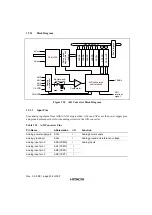
Страница 99: ...errupt Request Interrupt Request PS 2 External Bus Bus Interface Figure 8 1 Block Diagram of the Interrupt Controller 8 1 3 Pin Configuration Name Abbr I O Description Interrupt Request IRQ0 O Interrupt output to SH 4 SH7709 from the Intelligent Peripheral Controller 8 1 4 Register Configuration Name Abbr R W Initial Value Address Access Size Interrupt Request Register NIRR R W H 10005000 16 Inter...

Страница 100: ...e interrupt sources The interrupt sources will be recorded by the CPU The CPU will then determine the priority order and execute the interrupt service based on the determined priority order That is to say the interrupt service will be executed for the interrupt requests in the order from the highest priority to the lowest After the highest priority interrupt service is decided by the CPU the CPU w...

Страница 101: ...s bit represents PCMCIA0 interrupt request status 1 The interrupt request is generated from PCMCIA0 0 No interrupt requests are generated from PCMCIA0 13 PCMCIA1 interrupt request status PCC1R This bit represents PCMCIA1 interrupt request status 1 The interrupt request is generated from PCMCIA1 0 No interrupt requests are generated from PCMCIA1 12 AFE interrupt requests status AFER This bit repres...

Страница 102: ...re generated from IrDA 5 UART interrupt request status UARTR This bit represents UART0 interrupt request status 1 The interrupt request is generated from UART0 0 No interrupt requests are generated from UART0 4 Reserved 3 Parallel port interrupt request status PPR This bit represents Parallel port interrupt request status 1 The interrupt request is generated from Parallel port 0 No interrupt reque...

Страница 103: ... request from PS2 Keyboard is masked 0 The interrupt request from PS2 Keyboard is not masked 0 14 PCMCIA0 Interrupt Mask Control PCC0M This bit is used to control the mask option for PCMCIA0 interrupt request 1 The interrupt request from PCMCIA0 is masked 0 The interrupt request from PCMCIA0 is not masked 0 13 PCMCIA1 Interrupt Mask Control PCC1M This bit is used to control the mask option for PCM...

Страница 104: ...upt request from PS2 Mouse is not masked 0 6 IrDA Interrupt Mask Control IRDAM This bit is used to control the mask option for IrDA interrupt request 1 The interrupt request from IrDA is masked 0 The interrupt request from IrDA is not masked 0 5 UART Interrupt Mask Control UARTM This bit is used to control the mask option for UART0 interrupt request 1 The interrupt request from UART0 is masked 0 T...

Страница 105: ... R W R W R W R W Bit 7 6 5 4 3 2 1 0 Bit Name PS2MST IRDAT UARTT PPT SCDIT USBT ADCT Initial Value 0 0 0 0 0 0 0 R W R W R W R W R W R W R W R W Bit Description Default 15 PS2 Keyboard Interrupt Trigger Mode PS2KBT This bit is used to set the trigger mode for PS2 Keyboard interrupt request 1 The interrupt request from PS2 Keyboard is in edge trigger mode 0 The interrupt request from PS2 Keyboard i...

Страница 106: ...vel trigger mode 0 8 KBC Interrupt Trigger Mode KBCT This bit is used to set the trigger mode for KBC interrupt request 1 The interrupt request from KBC is in edge trigger mode 0 The interrupt request from KBC is in level trigger mode 0 7 PS2 Mouse Interrupt Trigger Mode PS2MST This bit is used to set the trigger mode for PS2 Mouse interrupt request 1 The interrupt request from PS2 Mouse is in edg...

Страница 107: ...quest from SCDI is in level trigger mode 0 1 USB Interrupt Trigger Mode USBT This bit is used to set the trigger mode for USB interrupt request 1 The interrupt request from USB is in edge trigger mode 0 The interrupt request from USB is in level trigger mode 0 0 ADC Interrupt Trigger Mode ADCT This bit is used to set the trigger mode for ADC interrupt request 1 The interrupt request from ADC is in...

Страница 108: ...be read or written to at any moment The counter constant is auto reloaded when reaching zero Supports binary counting Supports START STOP counting The input frequency of timer can be pre scaled the options are 1 1 4 1 8 1 16 Generates interrupt output timer1r timer0r to interrupt controller INTC when counter reaches zero Supports STANDBY mode which is able to stop the clock operation of the timer ...

Страница 109: ...KIO CPU BUS Interface Interrupt request DREQ1 TMO1 TMO0 timer1r timer0r Clock Scales 1 1 2 1 4 1 8 1 16 1 32 16 bit counter CKIO PWM1CS PWM0CS 16 bit counter TCVR1 TCVR0 TRVR1 TRVR0 TIRR TIDR PWM1LPC PWM1HPC PWM0LPC PWM0HPC CPU BUS Interface PWM1 PWM0 Figure 9 1 Block Diagram of Timer ...

Страница 110: ...ister Size Access Size Timer 1 constant value register TCVR1 H 10006000 16 16 Timer 0 constant value register TCVR0 H 10006002 16 16 Timer 1 read value register TRVR1 H 10006004 16 16 Timer 0 read value register TRVR0 H 10006006 16 16 Timer 1 control register TCR1 H 10006008 16 16 Timer 0 control register TCR0 H 1000600A 16 16 Timer interrupt request register TIRR H 1000600C 16 16 Timer interrupt ...

Страница 111: ... timer 1 The register is initialized to H FFFF at RESET Address H 10006000 Bit 15 14 13 12 11 10 9 8 Bit Name Initial Value 1 1 1 1 1 1 1 1 R W R W R W R W R W R W R W R W R W Bit 7 6 5 4 3 2 1 0 Bit Name Initial Value 1 1 1 1 1 1 1 1 R W R W R W R W R W R W R W R W R W Bit Description Default 15 0 These bits are set as the timer 1 constant value H FFFF ...

Страница 112: ...alue 1 1 1 1 1 1 1 1 R W R W R W R W R W R W R W R W R W Bit Description Default 15 0 These bits are set as the timer 0 constant value H FFFF 9 2 3 TRVR1 Timer 1 Read Value Register The TRVR1 a 16 bit register serves to read the counting value in the timer 1 This register would be reset to H 0002 when the timer is stopped Address H 10006004 Bit 15 14 13 12 11 10 9 8 Bit Name Initial Value R W R R ...

Страница 113: ...ounting value in timer 0 This register would be reset to H 0002 when the timer is stopped Address H 10006006 Bit 15 14 13 12 11 10 9 8 Bit Name Initial Value R W R R R R R R R R Bit 7 6 5 4 3 2 1 0 Bit Name Initial Value R W R R R R R R R R Bit Description Default 15 0 The timer 0 counter value is read from these bits ...

Страница 114: ... R W Bit Description Default 15 5 Reserved 0 4 This bit is used to enable the DMA request as timer 1 reaches zero 1 Enable the DMA request 0 Disable the DMA request 0 3 This bit is used to enable the timer 1 output TMO1 1 Output DMA request to port TMO1 0 Output DMA request to port DREQ1 0 2 1 These two bits are used for the pre scale option for the timer 1 The input clock for timer 1 is selected ...

Страница 115: ...cription Default 15 5 Reserved 0 4 This bit is used to enable the A D converter trigger signal ADTRIG as timer 0 reaches zero 1 Enable the ADTRIG signal 0 Disable the ADTRIG signal 0 3 This bit is used to enable the timer 0 output TMO0 1 Output ADTRIG to port TMO0 0 Output ADTRIG to internal ADC 0 2 1 These two bits are used for the pre scale option for the timer 0 The input clock for the timer 0 ...

Страница 116: ...tial Value 0 0 0 0 0 0 0 0 R W R W R W R W R W R W R W R W R W Bit Description Default 15 2 Reserved 0 1 This bit reflects the interrupt service request from the timer 1 This bit is set when counting value of the timer 1 reaches zero and it can be cleared by writing 0 to this bit 1 There is an interrupt request from the timer 1 0 There is no interrupt request from the timer 1 0 0 This bit reflects...

Страница 117: ...erved reserved reserved reserved reserved TMU1D TMU0D Initial Value 0 0 0 0 0 0 0 0 R W R W R W R W R W R W R W R W R W Bit Description Default 15 2 Reserved 0 1 This bit is used to disable the interrupt service request from the timer 1 1 The interrupt request from the timer 1 is disabled 0 The interrupt request from the timer 1 is enabled 0 0 This bit is used to disable the interrupt service requ...

Страница 118: ...iption Default 15 6 Reserved 5 0 PWM 1 Counting Clock Scale P1CS 5 0 These six bits provide six clock scale modes for PWM 1 width counting Only one bit will be active at the same time and the lower bit has higher priority while several bits are on at the same time B 000000 PWM 1 function is disabled B 000001 PWM 1 is counting with clock scale CKIO B 000010 PWM 1 is counting with clock scale CKIO 2...

Страница 119: ...t 15 14 13 12 11 10 9 8 Bit Name P1LC15 P1LC14 P1LC13 P1LC12 P1LC11 P1LC10 P1LC9 P1LC8 Initial Value 1 1 1 1 1 1 1 1 R W R W R W R W R W R W R W R W R W Bit 7 6 5 4 3 2 1 0 Bit Name P1LC7 P1LC6 P1LC5 P1LC4 P1LC3 P1LC2 P1LC1 P1LC0 Initial Value 1 1 1 1 1 1 1 1 R W R W R W R W R W R W R W R W R W Bit Description Default 15 0 PWM 1 Low Pulse Counter Value P1LC 15 0 These bits define the low pulse wid...

Страница 120: ...it 15 14 13 12 11 10 9 8 Bit Name P1HC15 P1HC14 P1HC13 P1HC12 P1HC11 P1HC10 P1HC9 P1HC8 Initial Value 1 1 1 1 1 1 1 1 R W R W R W R W R W R W R W R W R W Bit 7 6 5 4 3 2 1 0 Bit Name P1HC7 P1HC6 P1HC5 P1HC4 P1HC3 P1HC2 P1HC1 P1HC0 Initial Value 1 1 1 1 1 1 1 1 R W R W R W R W R W R W R W R W R W Bit Description Default 15 0 PWM 1 High Pulse Counter Value P1HC 15 0 These bits define the high pulse ...

Страница 121: ...ription Default 15 6 Reserved 5 0 PWM 0 Counting Clock Scale P0CS 5 0 These six bits provide six clock scale modes for PWM 0 width counting Only one bit will be active at the same time and the lower bit has higher priority while several bits are on at the same time B 000000 PWM 0 function is disabled B 000001 PWM 0 is counting with clock scale CKIO B 000010 PWM 0 is counting with clock scale CKIO ...

Страница 122: ...it 15 14 13 12 11 10 9 8 Bit Name P0LC15 P0LC14 P0LC13 P0LC12 P0LC11 P0LC10 P0LC9 P0LC8 Initial Value 1 1 1 1 1 1 1 1 R W R W R W R W R W R W R W R W R W Bit 7 6 5 4 3 2 1 0 Bit Name P0LC7 P0LC6 P0LC5 P0LC4 P0LC3 P0LC2 P0LC1 P0LC0 Initial Value 1 1 1 1 1 1 1 1 R W R W R W R W R W R W R W R W R W Bit Description Default 15 0 PWM 0 Low Pulse Counter Value P0LC 15 0 These bits define the low pulse wi...

Страница 123: ...R W Bit Description Default 15 0 PWM 0 High Pulse Counter Value P0HC 15 0 These bits define the high pulse width of PWM 0 H FFFF 9 3 Special Register Programming Sequence In general before setting the timer control registers TCR1 TCR0 to start counting the timer constant registers TCVR1 TCVR0 should be set first Otherwise the selected timer will start counting from H FFFF 9 4 Interrupt Timing The ...

Страница 124: ...timer1 0r timer1 0_clk n n n 1 0 Figure 9 2 Interrupt Request Timer1 0r Timing Diagram in Case Prescale 1 Timer1 0_clk CKIO CKIO timer1 0_clk IA ID 15 0 RD WR MWE1 0 timercs TRVR 1 0 timer1 0r 0 TMU1 0M TIRR Figure 9 3 Interrupt Request Timer1 0r Timing Diagram in Case Prescale 1 4 Timer1 0_clk CKIO 4 ...

Страница 125: ... TRVR 1 0 timer1 0r 0 TMU1 0M TIRR Figure 9 5 Interrupt Request Timer1 0r Timing Diagram in Case Prescale 1 16 Timer1 0_clk CKIO 16 9 5 A D Trigger Signal ADTRIG The A D trigger signal ADTRIG is enabled by the control bit EADT in TCR0 The pulse width of the A D trigger signal is sixteen cycles of CKIO to trigger the A to D converter Therefore the timer constant register TCVR0 should be properly se...

Страница 126: ..._clk TRVR1 0 ADTRIG 0 n n 1 n 2 Figure 9 7 A D Trigger Signal ADTRIG Timing Diagram in Case Prescale 1 4 Timer0_clk CKIO 4 CKIO timer1 0_clk TRVR1 0 ADTRIG 0 Figure 9 8 A D Trigger Signal ADTRIG Timing Diagram in Case Prescale 1 8 Timer0_clk CKIO 8 CKIO timer1 0_clk TRVR1 0 ADTRIG 0 n Figure 9 9 A D Trigger Signal ADTRIG Timing Diagram in Case Prescale 1 16 Timer0_clk CKIO 16 Note The transient de...

Страница 127: ...when the first cycle DRAK1 output is detected The DMA transfer is completed after it finishes transferring all the data transfers set in DMATCR 9 7 PWM Operation The PWM signal is generated while the proper value is written to the clock scale register PWMCS to activate the PWM generation function and decide the PWM width counting clock Based on the decide PWM width counting clock the PWM operating...

Страница 128: ...nnel1 PCC1 supports both of the IC memory card interface and I O Memory card interface Able to switch to an Attribute memory or a Common memory or an I O space via the CPU addresses Provides a segment bit an address bit for the PC card for the Common memory therefore a 64 MB space of full PCMCIA specifications can be accessed Provides a flexible power switch interface to either TPS2206 or MIC2563 ...

Страница 129: ... only register which reads the status of the PC card connected to PCC0 PCC0ISR is subject to the PC card status Bit Description Default 7 PCC0 Ready IREQ0 Pin Status P0READY IREQ0 If this bit is high Indicates that the value of pin PCC0RDY is 1 when the PC card connected to PCC0 is the IC memory card interface Indicates that the value of pin IREQ is 1 when the I O and Memory card interface is the ...

Страница 130: ...ted to PCC0 is 1 If this bit is low Indicates that the value of pin PCC0CD1 in the PC card connected to PCC0 is 0 IC Memory Interface 1 0 PCC0BVD2 SPKR0 Pin Status P0BVD2 SPKR0 PCC0BVD1 STSCHG0 Pin Status P0BVD1 STSCHG0 11 Indicates that the battery voltage state of the PC card connected to PCC0 is normal Battery Good 01 Indicates that the battery must be replaced although data integrity is guaran...

Страница 131: ...C0 Output Drive P0DRV If this bit is high enables the output interfaces to PCC0 If this bit is low tri states the output interfaces to PCC0 0 6 PCC0 PC Card Reset P0PCCR If this bit is high Sets a high level to reset pin PCC0RESET for the PC card connected to PCC0 If this bit is low Sets a low level to reset pin PCC0RESET for the PC card connected to PCC0 Initial value 0 5 PCC0 PC Card Type P0PCCT...

Страница 132: ...ing P0PA25 If this bit is high When the Common memory space is accessed for the PC card connected to PCC0 1 is output to pin PCC0A25 If this bit is low When the Common memory space is accessed for the PC card connected to PCC0 0 is output to pin PCC0A25 Initial value 0 1 PCC0A24 Pin Setting P0PA24 If this bit is high When bit P0MMOD is 1 and the Common memory space is accessed for the PC card conn...

Страница 133: ...ial value If bit 3 card detection enable in the PCC0 card status change interrupt enable register PCC0CSCIER is set to 1 a software card detect change interrupt can be generated by writing 1 to this bit If bit 3 card detection enable in the PCC0CSCIER is reset to 0 interrupts will not occur even when writing 1 to this bit 0 6 Power Switch Select PSWSEL Select power switch interface 0 MIC2563 1 TPS...

Страница 134: ...r to reset this bit to 0 This bit is not changed if 1 is written In this bit 0 is always read in the I O and Memory card interface 0 1 PCC0 Battery Warning P0BW If this bit is high Indicates that pins BVD2 and BVD1 in the PC card are in the battery warning state that the battery must be replaced although the data integrity is guaranteed when the PC card is in the IC memory card interface If this b...

Страница 135: ...is detected in PCC0 Initial value 0 6 5 PCC0 Interrupt Request Enable 1 P0IREQE1 PCC0 Interrupt Request Enable 0 P0IREQE0 00 Any kind of IREQ interrupt request signal is not accepted for the PC card connected to PCC0 Bit 5 in the status change register PCC0CSCR functions as a READ only bit and can indicate the status of the inversion signal of the IREQ pin Initial value 01 The level mode IREQ inte...

Страница 136: ...card connected to PCC0 regardless of the value of pin PCC0RDY Initial value 0 1 PCC0 Battery Warning Interrupt Enable P0BWE If this bit is high An interrupt occurs when pins PCC0BVD2 and PCC0BVD1 are in the state that the battery must be replaced although the data integrity is guaranteed If this bit is low No interrupt occurs when pins PCC0BVD2 and PCC0BVD1 are in the state that the battery must b...

Страница 137: ...are reset or in software based STANDBY mode Bit Description Default 7 5 Reserved 0 4 D8 SHDN bit of the TPS2206 0 3 PCC0 VPP Select 1 P0VPP1 If this bit is high set the voltage control pin P0VPP1 as high level If this bit is low set the voltage control pin P0VPP1 as low level 0 2 PCC0 VPP Select 0 P0VPP0 If the bit is high set the voltage control pin P0VPP0 as high level If this bit is low set the...

Страница 138: ...ption Default 7 D7 B_VCC5 bit of the TPS2206 0 6 D6 B_VCC3 bit of the TPS2206 0 5 D5 B_VPP_VCC bit of the TPS2206 0 4 D4 B_VPP_PGM bit of the TPS2206 0 3 D3 A_VCC3 bit of the TPS2206 0 2 D2 A_VCC5 bit of the TPS2206 0 1 D1 A_VPP_VCC bit of the TPS2206 0 0 D0 A_VPP_PGM bit of the TPS2206 0 10 4 7 PCC1 Interface Status Register PCC1ISR Bit 7 6 5 4 3 2 1 0 Bit Name P1READ Y IREQ1 P1MWP P1VS2 P1VS1 P1...

Страница 139: ...s low Indicates that the value of pin PCC1VS2 of the PC card connected to PCC1 is 0 4 PCC1VS1 Pin Status P1VS1 If this bit is high Indicates that the value of pin PCC1VS1 of the PC card connected to PCC1 is 1 If this bit is low Indicates that the value of pin PCC1VS1 in the PC card connected to PCC1 is 0 3 PCC1CD2 Pin Status P1CD2 If this bit is high Indicates that the value of pin PCC1CD2 in the ...

Страница 140: ...REG and sets the PC card type for the PC card connected to PCC1 PCC1GCR is initialized at power up reset and holds its value at software reset or in software based STANDBY mode Bit Description Default 7 PCC1 Output Drive P1DRV If this bit is high enables the output interfaces to PCC1 If this bit is low tri states the output interfaces to PCC1 0 6 PCC1 PC Card Reset P1PCCR If this bit is high Sets ...

Страница 141: ...25 Pin Setting P1PA25 If this bit is high When the Common memory space is accessed for the PC card connected to PCC1 1 is output to pin PCC1A25 If this bit is low When the Common memory space is accessed for the PC card connected to PCC1 0 is output to pin PCC1A25 Initial value 0 1 PCC1A24 Pin Setting P1PA24 If this bit is high When bit P1MMOD is 1 and the Common memory space is accessed for the P...

Страница 142: ...PCC1CSCIER is reset to 0 interrupts will not occur even when writing 1 to this bit 0 6 Reserved 5 PCC1 Interrupt Request P1IREQ If this bit is high Indicates that an interrupt request for the IREQ pin in the PC card has occurred when the PC card is in the I O and Memory card interface If this bit is low Indicates no interrupt requests occur for the IREQ pin in the PC card when the PC card is in th...

Страница 143: ...tery must be replaced although the data integrity is guaranteed when the PC card is in the IC memory card interface If this bit is low Indicates that pins BVD2 and BVD1 in the PC card are not in the battery warning state when the PC card is in the IC memory card interface Initial value This bit is updated when the BVD2 and BVD1 pins are changed Write 0 to bit 2 in order to reset this bit to 0 This...

Страница 144: ...gnal is not accepted for the PC card connected to PCC1 Bit 5 in the status change register PCC1CSCR functions as a READ only bit and indicates the status of the inversion signal of the IREQ pin Initial value 01 The level mode IREQ interrupt request signal is accepted for the PC card connected to PCC1 In the level mode an interrupt occurs when level 0 of the signal input from the IREQ pin is detect...

Страница 145: ...when pins PCC1BVD2 and PCC1BVD1 are in the state that the battery must be replaced although the data integrity is guaranteed If this bit is low No interrupt occurs when pins PCC1BVD2 and PCC1BVD1 are in the state that the battery must be replaced although the data integrity is guaranteed Initial value 0 0 PCC1 Battery Dead Interrupt Enable P1BDE If this bit is high An interrupt occurs when pins PC...

Страница 146: ...software based STANDBY mode Bit Description Default 7 4 Reserved 3 PCC1 VPP Select 1 P1VPP1 If this bit is high sets the voltage control pin P1VPP1 as high level If this bit is low sets the voltage control pin P1VPP1 as low level 0 2 PCC1 VPP Select 0 P1VPP0 If the bit is high sets the voltage control pin P1VPP0 as high level If this bit is low sets the voltage control pin P1VPP0 as low level 0 1 ...

Страница 147: ...Rev 3 0 03 01 page 128 of 390 ...

Страница 148: ...eeds are complied with Synchronous Data Link Control SDLC protocol a packet with start stop flags delimiting a data packet encoded by zero insertion The 4Mbit protocol uses an optical preamble and start stop flags to delimit the 4 Pulse Position Modulated 4 PPM packet data 11 1 1 Features Supports HPSIR or ASKIR infrared interface Supports MIR and FIR Provides DMA channel mode for FIR and DREQ0 is...

Страница 149: ...s data flow control from host to FIR MODEM It contains transmitting FIFO receiving FIFO and some registers to manage the FIFO operations The related registers will be described in the later section The FIR MODEM block contains the parallel data to from serial data logic This block also implements encoding the serial data to 4M mode bit stream The UART block is designed to be compatible with 16550 ...

Страница 150: ...HP SIR and SHARP ASK MODEM implements encoding serial data into bit stream for transmission decoding bit stream into serial data for data receiving For FIR transfer protocol the data flow is from host to FIR TX RV FIFO and to FIR MODEM 1 Host sets SIR Register ISIRR to FIR MODEM see FIR Controller registers description in section11 2 2 on the next page 2 Host writes data into TX FIFO for transmiss...

Страница 151: ... Control 0 x x x 1 1 H 10007002 H 10007004 H 10007006 H 10007008 H 10007000 H 10007002 IrIER Interrupt Enable Register IrIIR Interrupt Identification Register IrLCR Line Control Register IrMCR Modem Control Register IrDLL Divisor Latch LSB IrDLM Divisor Latch MSB IrIER IrFCR FIFO Control Register IrLCR IrMCR IrDLL IrDLM Status x x x H 1000700A H 1000700C H 1000700E IrLSR Line Status Register IrMSR...

Страница 152: ...e Count High Register IMSTCR Master Control register IFAR Address Register ITBCLR Tx Byte Count Low Register ITBCHR Tx Byte Count High Register 2 2 2 2 2 2 2 2 H 10007100 H 10007102 H 10007104 H 10007106 H 10007108 H 1000710A H 1000710C H 1000710E IMSTCR Master Control Register IIRC1R Infrared Configuration 1 Register IIRTCR Infrared Transceiver Control Register IIRC2R Infrared Configuration 2 Reg...

Страница 153: ...Interrupt Enable IEN Setting this bit to 1 enables all FIR Controller interrupts 0 6 Transmitter Enable TXEN Setting this bit to 1 enables the transmitter logic in the FIR Controller No packets are transmitted until the transmitter has been enabled 0 5 Receiver Enable RXEN Setting this bit to 1 enables the receiver logic in the FIR Controller No packets are received until the receiver has been ena...

Страница 154: ...lear the Rx interrupt condition Reading the Rx Ring Frame Counter Low Register Issuing a RESET Rx SPECIAL CONDITION INTERRUPT command Clearing the Rx Enable bit HARDWARE REST SOFTWARE RESET 3 1 Interrupt identification IID 2 0 These three bits correspond to interrupt identification ID2 ID0 which provide an alternative method for identifying the interrupt source by indicating the interrupt type and...

Страница 155: ... 0 DMA Channel for Transmit 1 1 Reserved 00 5 Reserved 4 Internal Loop back ILOOP When set to 1 the 4Mbit modem issues a transmit data output signal which is then internally looped back to its receive data input This allows for diagnostic testing of the modem transmit and receive data paths 0 3 0 Reserved 4 Rx FIFO Register IRFR Address H 10007104 Bank 0 Read Bit 7 6 5 4 3 2 1 0 Bit Name RD7 RD6 R...

Страница 156: ... TO SEND signal to the modem 0 6 Tx FIFO Ready interrupt Enable TFRIEN Setting this bit to 1 enables Tx FIFO Ready interrupts Setting this bit to 0 disables Tx FIFO Ready interrupts 0 5 Tx FIFO Underrun EOM Interrupt Enable TFUIEN Enables Tx FIFO Underrun EOM Interrupt Setting this bit to 1 enables FIFO underrun and EOM interrupts 0 4 Tx FIFO Threshold Level Control TFTL Setting this bit to 1 sets...

Страница 157: ...ng this bit to 0 causes the transmitter to transmit continuous flags 1Mbit mode or continuous preambles 4Mbit mode when the transmitter is idle 0 0 Underrun Abort UA Underrun Abort When a FIFO underrun occurs the software has two options before transmission is terminated One option is to send an abort sequence to the receiving end The other option is to transmit a CRC and an ending stop flag follo...

Страница 158: ...ommands the 4Mbit modem to send a SIR Interaction Pulse based on the bit setting A 01 bit setting instructs the 4Mbit modem to transmit a SIP at the end of current packet A 10 bit setting instructs the 4Mbit modem to transmit a SIP immediately regardless of the modem current activity Note SIP control bits are self clearing 00 3 Number of Starting Flags or Preambles NSFP Specifies the number of sta...

Страница 159: ...upt occurs immediately after the CRC and ending flag have been transmitted If bit 2 of Tx Control 1 Register Auto Reset EOM is enabled the EOM bit will automatically clear when Tx Status is read The EOM bit can also cleared by a RESET FIFO UNDERRUN LATCH command from the Reset Command Register 0 1 Tx FIFO Ready TFRDY When set to 1 indicates Tx FIFO is ready for more data transfers When the bit 6 o...

Страница 160: ...is bit results in no CRC errors being reported 1 5 4 RX Address Mode RADM 1 0 Specify the type of address filtering to apply for determining which receive frames to accept b5 b4 Rx Address Mode 0 0 All packets accepted 0 1 Address must match Frame Address Register FAR 1 0 Address high nibble must match FAR 1 1 Reserved Note Packets with a universal address 0x7F are always accepted 00 3 Sync Hunt C...

Страница 161: ... of Frame EOF When set to 1 indicates an ending stop flag or abort sequence was detected in the incoming data stream This bit is automatically cleared upon detection of the beginning start flag of the next incoming packet 3 RX FIFO Empty RFEM When set to 1 indicates Rx FIFO is not empty When set to 0 indicates Rx FIFO is empty When this bit is set it does not cause an interrupt rather it is used t...

Страница 162: ...ition Interrupt 0 1 0 0 Reset Rx Ring Frame Pointer 0 1 0 1 Reset FIFO Underrun EOM Latch 0 1 1 0 Reset Tx FIFO Pointer 0 1 1 1 Hardware Reset Note These bits are self clearing i e a programmer does not need to reset the RESET Command bit value to 0000 3 0 Reserved 12 Frame Address Register IFAR Address H 10007102 Bank 1 Read Write Bit 7 6 5 4 3 2 1 0 Bit Name RFA7 RFA6 RFA5 RFA4 RFA3 RFA2 RFA1 In...

Страница 163: ...ta being received It is useful when receiving back to back packets Bit 7 6 5 4 3 2 1 0 Bit Name D7 D6 D5 D4 D3 D2 D1 D0 14 Rx Byte Count High Register IRBCHR Address H 10007106 Bank 1 Read Bit 7 6 5 4 3 2 1 0 Bit Name RBC12 RBC11 RBC10 RBC9 RBC8 Initial Value R W R R R R R Bit Description Default 7 5 Reserved 4 0 Rx Byte Count D8 D12 Provides a running count high order value of the number of bytes...

Страница 164: ...3 2 1 0 Bit Name D7 D6 D5 D4 D3 D2 D1 D0 The RFP value is initially set to 0000h Thus before receiving the first packet software should not use the RFP value for any computation 16 Rx Ring Frame Pointer High Register IRRFPHR Address H 1000710A Bank 1 Read Bit 7 6 5 4 3 2 1 0 Bit Name RFP15 RFP14 RFP13 RFP12 RFP11 RFP10 RFP9 RFP8 Initial Value R W R R R R R R R R Bit Description Default 7 0 Ring Fr...

Страница 165: ...ster with the low order byte length of the data packet When the counter reaches zero the transmitter ceases to make DMA requests Transmission continues until Tx FIFO is depleted Bit 7 6 5 4 3 2 1 0 Bit Name D7 D6 D5 D4 D3 D2 D1 D0 18 Tx Byte Count High Register ITBCHR Address H 1000710E Bank 1 Read Write Bit 7 6 5 4 3 2 1 0 Bit Name TBC12 TBC11 TBC10 TBC9 TBC8 Initial Value 1 0 0 0 0 R W R W R W R...

Страница 166: ... W R W R W R W R W R W R W Bit Description Default 7 4 Infrared Speed IRSPD 3 0 Specify the data rate under 1Mbit FIR modulation B7 b6 b5 b4 Infrared Speed 0 0 0 0 1 152 Mbps 0 0 0 1 0 756 Mbps 0 0 1 0 0 288 Mbps 0000 3 0 Infrared Modulation IRMOD 3 0 Specify the modulation mode of infrared communication b3 b2 b1 b0 Infrared Modulation 0 0 0 0 HP SIR 0 0 0 1 Sharp ASK 0 0 1 0 1 152 Mbps IrDA 0 0 1...

Страница 167: ...s bit will be invalidated 4 Mode Select MODSEL When an IBM like transceiver is selected in the configuration register mode select function will be present on the MODSEL pin Setting this bit to 1 causes the external MODSEL pin to be high Setting this bit to 0 causes the external MODSEL pin to be low When an HP like transceiver is selected in the configuration register this bit will be invalidated 3...

Страница 168: ...ansceiver and is not recommended for normal operation where pulse widths can vary significantly The setting and their effects are Autochop Enable CCTRL1 CCTRL0 Effect 000 Chopping circuit is disabled 001 Extend the single pulse width tolerance to 187ns Back to back pulses must be greater than 209ns 010 Extend the single pulse width tolerance to 229ns Back to back pulses must be greater than 249ns ...

Страница 169: ...uration 3 Register IIRC3R Address H 1000710A Bank 2 Read Write Bit 7 6 5 4 3 2 1 0 Bit Name SCDIEN SCD TMIEN TMI Initial Value 0 0 0 0 R W R W R W R W R W Bit Description Default 7 Enables Sharp CD Interrupt SCDIEN Setting this bit to 1 enables Sharp Carrier Detect interrupts 6 Sharp Carrier Detect SCD When set to 1 this READ only status bit indicates a 500KHz Sharp ASK carrier has been detected T...

Страница 170: ...supports 4M mode and uses IRCLK 48MHz clock 1 25 FIR Configuration Register IFIRCR Address H 100071E0 Read Write Bit 7 6 5 4 3 2 1 0 Bit Name RX2_PP RX_PP TMODE Initial Value 0 0 0 R W R W R W R W Bit Description Default 7 3 Reserved 0 2 RX2 Pull_up RX2_PP Setting this bit to 1 enables the pull up function for MODSEL RX2 Setting this bit to 0 disables the pull up function for MODSEL RX2 0 1 RX Pul...

Страница 171: ...Default 7 3 Reserved 0 0 2 Timing Control TMCR 2 0 These three bits TMCR 2 0 are used to adjust the timing for different CKIO frequency rates 3 b000 3 b001 Set as CKIO frequency is 12 5MHz 3 b010 Set as CKIO frequency is 25MHz 3 b011 Set as CKIO frequency is 30MHz 3 b100 Set as CKIO frequency is 40MHz 3 b101 Set as CKIO frequency is 50MHz 3 b110 Set as CKIO frequency is 66MHz 3 b111 Reserved ...

Страница 172: ...RTS TFRIEN TFUIEN TFTL ADRTS TIDL and UA in ITC1R to start to transmit data RTS is used to activate the REQUEST TO SEND and start transmission TFRIEN enables Tx FIFO Ready interrupt request TFUIEN enables Tx FIFO underrun EOM interrupt request and TFTL controls Tx FIFO Threshold level ADRTS automatically deactives the REQUEST TO SEND TIDL controls Tx Idle state and UA specifies the FIFO underrun s...

Страница 173: ...n Receiving logic facilities 1 Receive control circuitry 2 Rx Byte Count Register to keep track of received bytes 3 Rx FIFO 16 x 11 bits 8 bit data 3 bit status Frame Error Abort and End Of Frame 4 Rx Ring Frame Counter to keep track of the Rx byte number in the host Rx buffer 5 Rx Ring Frame Pointer which points to the last byte of the last received packet in the host Rx buffer T1 Setup Phase 1 S...

Страница 174: ...or the next Start flag and another address match T4 Data Receiving 1 When a data byte is received the data and the three status bits are stored in the Rx FIFO 2 If DMA is enabled DMA request is activated when the FIFO threshold level is reached DMA request continues until all data stored in the FIFO have been transferred to the host receive buffer However the three status bits in the FIFO will not...

Страница 175: ...rame is required 6 The host reads IRSR to check for receive completion status 11 5 Example of Initialization and Programming Procedure for HP SIR 1 Enable HP SIR For HP SIR SHARP ASK and 4M mode FIR use 48 MHz clock 1 Set BKSEL 4 0 to select Bank 2 register Set 02h to IMSTCR 2 Set IRMOD 3 0 in IIRC1R to select HP SIR mode Set 00h to IIRC1R 3 Set SIRMOD in ISIRR to select FIR MODEM Set 00h to ISIRR...

Страница 176: ...or no parity and privileged interrupts The HD64465 provides two UART ports 12 2 Features Programmable FIFO or character mode In FIFO mode 16 byte FIFO buffer on the transmitter and receiver Add or delete standard asynchronous communication bits start stop parity to or from serial data The programmable Baud rate generator allows the division of input clock by 1 to 216 1 and generates internal 16X c...

Страница 177: ...em Status Register USCR Scratch Pad Register ULSR UMSR USCR Notes 1 DLAB is bit 7 of the Line Control Register 2 UART0 base address H 10008000 12 3 1 Data Register UTBR and URBR each hold from five to eight data bits If the transmitted data is less than eight bits it aligns to the LSB Either received or transmitted data is buffered by a shift register and is latched first by a holding register The...

Страница 178: ...Register Empty Interrupt 0 0 Sets this bit high to enable the Received Data Available Interrupt and Time out Interrupt in the FIFO mode 0 2 UIIR READ only This register facilitates the host CPU to determine interrupt priority and its source The priority of four existing interrupt levels is as follows 1 Received Line Status highest priority 2 Received Data Ready 3 Transmitter Holding Register Empty...

Страница 179: ...acter times and there is at least 1 character in it at this time URBR READ 0 0 1 0 Third Transmitter Holding Register Empty Transmitter Holding Register Empty UIIR READ if THRE is the Interrupt Source or THR write 0 0 0 0 Fourth Modem Status CTS DSR RI DCD UMSR READ Note X Not Defined Bit Description Default 7 6 Are set when UFCR 0 1 5 4 Always logic 0 0 3 In non FIFO mode this bit is a logic 0 In...

Страница 180: ...n this bit is cleared to low This bit has to be a logic 1 if the other bits of the UFCR are written to or they will not be properly programmed When this register changes to non FIFO mode all contents will be cleared 4 Divisor Latches READ WRITE There are two 8 bit Divisor Latches UDLL and UDLM which store the divisor in a 16 bit binary format They are loaded during initialization to generate a des...

Страница 181: ...ng read or write operations It must be set low to access the Data Register URBR and UTBR or the Interrupt Enable Register 6 Break Control Forces the Serial Output SOUT to the spacing state logic 0 by a logic 1 and this state will remain until a low level resetting ULCR 6 enabling the serial port to alert the terminal in a communication system 5 Stick Parity Bit When this bit and ULCR 3 are high at...

Страница 182: ... first regardless of the number used in transmission 1 0 Bit 0 Word Length Select Bit 0 WLS 0 Bit 1 Word Length Select Bit 1 WLS 1 Specify the number of bits in each serial character encoded as the following ULCR 1 ULCR 0 Word Length 0 0 5 bits 0 1 6 bits 1 0 7 bits 1 1 8 bits 7 UMCR READ WRITE Controls the interface with the modem or data set or device emulating a modem Table 12 4 Modem Control R...

Страница 183: ...on Default 7 In 16450 mode this bit is always 0 In the FIFO mode it is set high when there is at least one parity error framing or break interrupt in the FIFO This bit is cleared when the CPU reads ULSR if there are no subsequent errors in the FIFO 0 6 This READ only bit indicates that the Transmitter Holding Register and Transmitter Shift Register are both empty otherwise this bit is 0 It has the...

Страница 184: ...FO is full and the next character has been completely received by the Shift Register It will be reset when the SR is read by CPU 0 Data Ready DR bit logic 1 which indicates a character has been received by URBR and logic 0 indicating all of the data in URBR or RCV FIFO has been read Table 12 5 Line Status Register Bits LSR Bits Logic 1 Logic 0 LSR 7 PE FE BI FIFO mode LSR 6 Transmitter Empty TEMT ...

Страница 185: ...d CTS Indicates the complement of CTS input If the serial channel is in the loop mode bit 4 of UMCR is 1 this bit is equivalent to RTS in the UMCR 3 Delta Data Carrier Detect DDCD Indicates that the DCD input state has been changed since the last time read by the Host 2 Trailing Edge of Ring Indicator TERI Indicates that the RI input state to the serial channel has been changed from a low to high ...

Страница 186: ...emory and logic elements Before resetting UART remains in the idle mode until programmed Table 12 7 Reset Control of Register and Pinout Signals Register Signal Reset Control Reset Status Interrupt Enable Register Interrupt Identification Register FIFO Control Register Line Control Register Modem Control Register Line Status Register Modem Status Register SOUT RTS DTR Reset Reset Reset Reset Reset...

Страница 187: ...16550 The following is standard 16550 compatible component register access sequence For access URBR UTBR 1 Set bit 7 of the ULCR register to 0 2 Access URBR UTBR For Access UIER 1 Set bit 7 of the ULCR register to 0 2 Access UIER For Access UDLL UDLM 1 Set bit 7 of the ULCR register to 1 2 Access UDLL UDLM 12 6 Software Reset This method allows returning to a completely known state without a syste...

Страница 188: ...nd the most recent Host read from the FIFO is longer than four 4 consecutive character times b The time out timer will be reset after receiving a new character or after the Host reads the RCVR FIFO whenever any time out interrupt occurs The timer will be reset when the Host reads one character from the RCVR FIFO 2 XMIT Interrupt By setting the bit 0 of UFCR and the bit 1 of UIER to high the XMIT F...

Страница 189: ...e high whenever the RCVR FIFO contains at least one byte LSR 1 LSR 4 Specifies that errors have occurred Character error status is handled the same way as that in the interrupt mode The IIR is not affected since IER 2 0 LSR 5 The XMIT FIFO empty indication LSR 6 XMIT FIFO and Shift register empty LSR 7 RCVR FIFO error indication There is no trigger level reached or time out condition indicated in ...

Страница 190: ...v1 9 compliant High speed mode ECP IEEE 1284 compliant Backdrive current reduction Printer power on damage reduction No DMA mode is supported in ECP mode 13 3 Parallel Port Register Description Host Connector Pins SPP EPP ECP 1 STB WRITE nStrobe 2 9 PD0 PD7 PD0 PD7 PD0 PD7 10 ACK INTR nAck 11 BUSY WAIT Busy PeriphAck 2 12 PE NU 1 Perro nAckReverse 2 13 SLCT NU 1 Select 14 AFD DSTB nAutoFd HostAck ...

Страница 191: ...cr H 1000A004 8 8 Parallel Port Data FIFO cFifo H 1000A010 8 8 Test FIFO tFifo H 1000A010 8 8 Configuration Register A cnfgA H 1000A010 8 8 Configuration Register B cnfgB H 1000A012 8 8 Extended Control Register ecr H 1000A014 8 8 Table 13 2 Bit Map of the EPP Registers Register Address I O D0 D1 D2 D3 D4 D5 D6 D7 Mode Data Port H 1000A000 R W PD0 PD1 PD2 PD3 PD4 PD5 PD6 PD7 SPP EPP Status Port H ...

Страница 192: ...ans that an error has been detected 2 1 Reserved These bits are always 1 when read 11 0 TMOUT This bit is valid only in EPP mode and indicates that a 10 ms time out has occurred in EPP operation If in other mode this bit is always logic 1 when read 3 Control Port Register This register provides all output signals to control the printer The register can be read and written Table 13 4 Control Port R...

Страница 193: ...implemented in both forward and reverse directions to smooth data flow and improve the maximum bandwidth requirement The port supports an automatic handshaking for the standard parallel port to improve compatibility and increase the speed of mode transfer It also supports run length encoded RLE decompression in hardware Compression is accomplished by counting identical bytes and transmitting an RL...

Страница 194: ...the value on the PD bus instead of the value of the data register 010 Parallel Port FIFO Mode This mode is similar to the 000 mode except that the Host writes the data bytes to the FIFO The FIFO data is then automatically sent to the peripheral using the standard parallel port protocol This mode is only valid in the forward direction dcr 5 0 011 ECP Parallel Port Mode In the forward direction byte...

Страница 195: ...t pin 1 3 nFault The state of the nFault input pin 1 2 0 Reserved These bits are always 1 111 4 Device Control Register dcr Address H 1000A004 Mode All Address H 1000A004 Mode All Bit 7 6 5 4 3 2 1 0 Bit Name Reserved Reserved PDDIR IRQE SelectIn nlnit AutoFd Strobe Initial Value 1 1 0 0 0 0 0 R W R W R W R W R W R W R W R W R W Bit Description Default 7 6 Reserved These bits are always 1 11 5 PDD...

Страница 196: ...ction Data in this FIFO will be displayed on the PD bus without using hardware protocol handshaking The tFifo will not accept new data after it is full Performing a READ from an empty fFifo causes the last data byte to return 8 Configuration Register A cnfgA Address H 1000A010 Mode 111 This register is a read only register When read the returned data is valued at 10h it indicates to the system tha...

Страница 197: ...and cannot accept another byte 0 The FIFO has one free data byte space at least 0 0 Empty 1 The FIFO is empty 0 The FIFO contains at least one data byte 1 11 Mode Switching Operation In programmed I O control mode 000 or 001 P1284 negotiation and all other tasks happening before data is transferred and are controlled by software Setting mode to 011 or 010 will cause the hardware to perform an auto...

Страница 198: ...ets direction to one or zero and finally switches mode to 001 If the direction is set to 1 the hardware performs a handshaking form each ECP data byte READ and tries to fill the FIFO At this time Pwords may be read from the expDFifo while it retains data It is also possible for the hardware to performs ECP transfers by handshaking with individual bytes under program control in mode 001 or 000 even...

Страница 199: ...Rev 3 0 03 01 page 180 of 390 ...

Страница 200: ...functions of the interface are transmitting D A data from system to CODEC and receiving A D data from CODEC to system 14 1 1 Features Support for CS4218 CS4271 and AC97 Version1 03 and 2 0 CODECs Full duplex data transfer between CODEC and this interface Both PIO and DMA modes are supported for communication with system Provides SM3 Slave mode for communication with CS4218 or CS4271 and SM3 Master...

Страница 201: ...Diagram CSxx TX Controller AC97 RX Controller AC97 TX Controller CSxx RX Controller CODEC Chip Internal Bus Internal Bus Interface MISC Ckgen ACCLK SDOUT SDIN SSYNC ACIRQ ACPD ACRST SIBCLK Figure 14 1 The Block Diagram of Serial CODEC Interface ...

Страница 202: ...r Management Event has happened ACRST O Reset This pin when low resets the CS4218 to a known state 14 2 Register Description This Serial CODEC interface contains registers shown in the table below Table 14 2 Registers of SCDI Register or Buffer Function Access Size Address TDR Transmit Data Register for CS4218 or CS4271 32 bits H 1000C000 RDR Receive Data Register for CS4218 or CS4271 32 bits H 10...

Страница 203: ...ts H 1000C058 ARSR AC97 RX Status Register 32 bits H 1000C05C ACR AC97 Control Register 32 bits H 1000C060 ATAGR AC97 TAG Register 32 bits H 1000C064 SRAR Slot Request Active Register 16 bits H 1000C068 14 2 1 Transmit Data Register TDR TDR a 32 bit Write only register is used as a channel to write data to TX FIFO TDR is not initialized Bit 31 30 29 28 27 10 9 8 Bit Name TD31 TD30 TD29 TD28 TD27 T...

Страница 204: ...channel to read data from RX FIFO RDR is not initialized Bit 31 30 29 28 27 26 25 24 Bit Name RD31 RD30 RD29 RD28 RD27 RD26 RD25 RD24 Initial Value 0 0 0 0 0 0 0 0 R W R R R R R R R R Bit 23 22 21 20 19 18 17 16 Bit Name RD23 RD22 RD21 RD20 RD19 RD18 RD17 RD16 Initial Value 0 0 0 0 0 0 0 0 R W R R R R R R R R Bit 15 14 13 12 11 10 9 8 Bit Name RD15 RD14 RD13 RD12 RD11 RD10 RD9 RD8 Initial Value 0 ...

Страница 205: ...Value 0 0 0 0 0 0 0 0 R W R W R W R W R W R W R W R W R W Bit Description Default 15 14 Reserved 13 DMA mode Enable DMAEN If this bit is set to 1 DMA mode for CS4218 or CS4271 is enabled 0 12 Select CS4218 SL18 If this bit is set to 1 CS4218 interface is selected Otherwise CS4271 interface is selected 0 11 Cold Reset for AC97 CDRT Writes 1 to this bit will cause Cold AC97 Reset This bit is always ...

Страница 206: ... done interrupt and the control of transmit data path 0 Disabled 0 1 Flush RX FIFO FRF Setting this bit will flush RX FIFO and reset the RX FIFO pointer Always read 0 0 0 RX Enable RXEN 1 Enables RX done interrupt and the control of receive data path 0 Disabled 0 14 2 4 Status Register SR SR is a 16 bit Read only register that is used to reflect the status of this Serial CODEC Interface when the C...

Страница 207: ...riting 1 to this bit will clear this bit 0 8 TX Done Interrupt TDI 1 indicates that one block of Transmitting FIFO has been written to CODEC Writing 1 to this bit will clear this bit 0 7 6 Reserved 5 RX FIFO Not Empty Flag RNE 0 RX FIFO is empty 1 RX FIFO is not empty 0 4 3 RX FIFO Status RFS RFS 1 0 FIFO 1 FIFO 0 00 not full not full 01 not full full 10 full not full 11 full full 0 2 RX FIFO unde...

Страница 208: ... is not initialized in STANDBY mode Bit 15 14 13 12 11 10 9 8 Bit Name reserved reserved reserved reserved reserved reserved reserved reserved Initial Value 0 0 0 0 0 0 0 0 R W Bit 7 6 5 4 3 2 1 0 Bit Name reserved reserved reserved reserved reserved FS2 FS1 FS0 Initial Value 0 0 0 0 0 0 0 0 R W R W R W R W Bit Description Default 15 3 Reserved 0 2 0 Frequency Select FS 000 8kHz Frequency Sample R...

Страница 209: ...5 CA4 SA4 Initial Value 0 0 0 0 R W R W R W R W R W Bit 15 14 13 12 11 10 9 8 Bit Name CA3 SA3 CA2 SA2 CA1 SA1 CA0 SA0 Initial Value 0 0 0 0 0 0 0 0 R W R W R W R W R W Bit 7 6 5 4 3 2 1 0 Bit Name Initial Value 0 0 0 0 0 0 0 0 R W Bit Description Default 31 20 Reserved 19 Read Write Command RW 1 read 0 write 0 18 12 Control Register Address 6 0 CA6 CA0 Status Address 6 0 SA6 SA0 When this registe...

Страница 210: ...R W R W R W Bit 15 14 13 12 11 10 9 8 Bit Name CD11 SD11 CD10 SD10 CD9 SD9 CD8 SD8 CD7 SD7 CD6 SD6 CD5 SD5 CD4 SD4 Initial Value 0 0 0 0 0 0 0 0 R W R W R W R W R W R W R W R W R W Bit 7 6 5 4 3 2 1 0 Bit Name CD3 SD3 CD2 SD2 CD1 SD1 CD0 SD0 Initial Value 0 0 0 0 0 0 0 0 R W R W R W R W R W Bit Description Default 31 20 Reserved 19 4 Command Status Data 15 0 CD15 0 When this register is written th...

Страница 211: ...0 0 0 0 R W R W R W R W R W Bit 15 14 13 12 11 10 9 8 Bit Name D15 D14 D13 D12 D11 D10 D9 D8 Initial Value 0 0 0 0 0 0 0 0 R W R W R W R W R W R W R W R W R W Bit 7 6 5 4 3 2 1 0 Bit Name D7 D6 D5 D4 D3 D2 D1 D0 Initial Value 0 0 0 0 0 0 0 0 R W R W R W R W R W R W R W R W R W Bit Description Default 31 20 Reserved 19 0 Data 19 0 D19 0 When this register is written PCM Playback Left Channel Data w...

Страница 212: ...Initial Value 0 0 0 0 R W R W R W R W R W Bit 15 14 13 12 11 10 9 8 Bit Name D15 D14 D13 D12 D11 D10 D9 D8 Initial Value 0 0 0 0 0 0 0 0 R W R W R W R W R W R W R W R W R W Bit 7 6 5 4 3 2 1 0 Bit Name D7 D6 D5 D4 D3 D2 D1 D0 Initial Value 0 0 0 0 0 0 0 0 R W R W R W R W R W R W R W R W R W Bit Description Default 31 20 Reserved 19 0 Data 19 0 D19 0 When this register is written these bits will be...

Страница 213: ...0 0 0 R W R W R W R W R W Bit 15 14 13 12 11 10 9 8 Bit Name D15 D14 D13 D12 D11 D10 D9 D8 Initial Value 0 0 0 0 0 0 0 0 R W R W R W R W R W R W R W R W R W Bit 7 6 5 4 3 2 1 0 Bit Name D7 D6 D5 D4 D3 D2 D1 D0 Initial Value 0 0 0 0 0 0 0 0 R W R W R W R W R W R W R W R W R W Bit Description Default 31 20 Reserved 19 0 Data 19 0 D19 0 When this register is written these bits will be written to the ...

Страница 214: ...ue 0 0 0 0 R W R W R W R W R W Bit 15 14 13 12 11 10 9 8 Bit Name D15 D14 D13 D12 D11 D10 D9 D8 Initial Value 0 0 0 0 0 0 0 0 R W R W R W R W R W R W R W R W R W Bit 7 6 5 4 3 2 1 0 Bit Name D7 D6 D5 D4 D3 D2 D1 D0 Initial Value 0 0 0 0 0 0 0 0 R W R W R W R W R W R W R W R W R W Bit Description Default 31 20 Reserved 19 0 Data 19 0 D19 0 When this register is written these bits will be written to...

Страница 215: ...4 Bit Name Initial Value R W Bit 23 22 21 20 19 18 17 16 Bit Name D19 D18 D17 D16 Initial Value 0 0 0 0 R W W W W W Bit 15 14 13 12 11 10 9 8 Bit Name D15 D14 D13 D12 D11 D10 D9 D8 Initial Value 0 0 0 0 0 0 0 0 R W W W W W W W W W Bit 7 6 5 4 3 2 1 0 Bit Name D7 D6 D5 D4 D3 D2 D1 D0 Initial Value 0 0 0 0 0 0 0 0 R W W W W W W W W W Bit Description Default 31 20 Reserved 19 0 Data 19 0 D19 0 When t...

Страница 216: ...5 24 Bit Name Initial Value R W Bit 23 22 21 20 19 18 17 16 Bit Name D19 D18 D17 D16 Initial Value 0 0 0 0 R W W W W W Bit 15 14 13 12 11 10 9 8 Bit Name D15 D14 D13 D12 D11 D10 D9 D8 Initial Value 0 0 0 0 0 0 0 0 R W W W W W W W W W Bit 7 6 5 4 3 2 1 0 Bit Name D7 D6 D5 D4 D3 D2 D1 D0 Initial Value 0 0 0 0 0 0 0 0 R W W W W W W W W W Bit Description Default 31 20 Reserved 19 0 Data 19 0 D19 0 Whe...

Страница 217: ... Value R W Bit 23 22 21 20 19 18 17 16 Bit Name D19 D18 D17 D16 Initial Value 0 0 0 0 R W W W W W Bit 15 14 13 12 11 10 9 8 Bit Name D15 D14 D13 D12 D11 D10 D9 D8 Initial Value 0 0 0 0 0 0 0 0 R W W W W W W W W W Bit 7 6 5 4 3 2 1 0 Bit Name D7 D6 D5 D4 D3 D2 D1 D0 Initial Value 0 0 0 0 0 0 0 0 R W W W W W W W W W Bit Description Default 31 20 Reserved 19 0 Data 19 0 D19 0 When this register is wr...

Страница 218: ... Value 0 0 0 0 R W R W R W R W R W Bit 15 14 13 12 11 10 9 8 Bit Name D15 D14 D13 D12 D11 D10 D9 D8 Initial Value 0 0 0 0 0 0 0 0 R W R W R W R W R W R W R W R W R W Bit 7 6 5 4 3 2 1 0 Bit Name D7 D6 D5 D4 D3 D2 D1 D0 Initial Value 0 0 0 0 0 0 0 0 R W R W R W R W R W R W R W R W R W Bit Description Default 31 20 Reserved 19 0 Data 19 0 D19 0 When this register is written these bits will be writte...

Страница 219: ...e 0 0 0 0 R W R W R W R W R W Bit 15 14 13 12 11 10 9 8 Bit Name D15 D14 D13 D12 D11 D10 D9 D8 Initial Value 0 0 0 0 0 0 0 0 R W R W R W R W R W R W R W R W R W Bit 7 6 5 4 3 2 1 0 Bit Name D7 D6 D5 D4 D3 D2 D1 D0 Initial Value 0 0 0 0 0 0 0 0 R W R W R W R W R W R W R W R W R W Bit Description Default 31 20 Reserved 19 0 Data 19 0 D19 0 When this register is written these bits will be written to ...

Страница 220: ...alue 0 0 0 0 R W R W R W R W R W Bit 15 14 13 12 11 10 9 8 Bit Name D15 D14 D13 D12 D11 D10 D9 D8 Initial Value 0 0 0 0 0 0 0 0 R W R W R W R W R W R W R W R W R W Bit 7 6 5 4 3 2 1 0 Bit Name D7 D6 D5 D4 D3 D2 D1 D0 Initial Value 0 0 0 0 0 0 0 0 R W R W R W R W R W R W R W R W R W Bit Description Default 31 20 Reserved 19 0 Data 19 0 D19 0 When this register is written these bits will be written ...

Страница 221: ... 0 0 0 0 0 0 0 R W R W R W R W R W R W R W R W R W Bit 15 14 13 12 11 10 9 8 Bit Name PLSTFO VIE PRSTFO VIE PLFETFO VIE L2TFOVI E HTTFOVI E IOCTFOV IE PLTFUNI E PRTFUNI E Initial Value 0 0 0 0 0 0 0 0 R W R W R W R W R W R W R W R W R W Bit 7 6 5 4 3 2 1 0 Bit Name L1TFUNI E PCTFUNI E PLSTFU NIE PRSTFU NIE PLFETFU NIE L2TFUNI E HTTFUNI E IOCTFUN IE Initial Value 0 0 0 0 0 0 0 0 R W R W R W R W R W...

Страница 222: ...le L2TFRQIE When this bit is 1 Line 2 TX FIFO Request is enabled When this bit is 0 Line 2 TX FIFO Request is disabled 0 21 HSET TX FIFO REQUEST Interrupt Enable HTTFRQIE When this bit is 1 HSET TX FIFO Request is enabled When this bit is 0 HSET TX FIFO Request is disabled 0 20 IO CTRL TX FIFO REQUEST Interrupt Enable IOCTFRQIE When this bit is 1 IO CTRL TX FIFO Request is enabled When this bit is...

Страница 223: ...nterrupt Enable IOCTFOVIE When this bit is 1 IO CTRL TX FIFO OVERRUN Interrupt is enabled When this bit is 0 IO CTRL TX FIFO OVERRUN Interrupt is disabled 0 9 PCML TX FIFO UNDERRUN Interrupt Enable PLTFUNIE When this bit is 1 PCML TX FIFO UNDERRUN Interrupt is enabled When this bit is 0 PCML TX FIFO UNDERRUN Interrupt is disabled 0 8 PCMR TX FIFO UNDERRUN Interrupt Enable PRTFUNIE When this bit is...

Страница 224: ...bled 0 0 IO CTRL TX FIFO UNDERRUN Interrupt Enable IOCTFUNIE When this bit is 1 IO CTRL TX FIFO UNDERRUN Interrupt is enabled When this bit is 0 IO CTRL TX FIFO UNDERRUN Interrupt is disabled 0 14 2 19 AC97 TX FIFO Status Register ATSR a 32 bit Read Only register is used to reflect the status of AC97 TX controller Bits 31 30 are reserved The other bits are initialized to 0 at reset ATIER is not in...

Страница 225: ... by the system 0 24 PCMRS TX FIFO REQUEST PRSTFRQ 1 indicates that half of PCMRS TX FIFO is empty and must be filled by the system 0 23 PCMLFE TX FIFO REQUEST PLFETFRQ 1 indicates that half of PCMLFE FIFO is empty and must be filled by the system 0 22 Line2 TX FIFO REQUEST L2TFRQ 1 indicates that half of Line2 FIFO is empty and must be filled by the system 0 21 HSET TX FIFO REQUEST HTTFRQ 1 indica...

Страница 226: ...ML TX FIFO is underrun 0 8 PCMR TX FIFO UNDERRUN PRTFUN 1 indicates that PCMR TX FIFO is underrun 0 7 Line 1 TX FIFO UNDERRUN L1TFUN 1 indicates that Line1 FIFO is underrun 0 6 PCMC TX FIFO UNDERRUN PCTFUN 1 indicates that PCMC TX FIFO is underrun 0 5 PCMLS TX FIFO UNDERRUN PLSTFUN 1 indicates that PCMLS TX FIFO is underrun 0 4 PCMRS TX FIFO UNDERRUN PRSTFUN 1 indicates that PCMRS TX FIFO is under...

Страница 227: ... 12 11 10 9 8 Bit Name HTRFRQI E IOCSRFR QIE PLRFOVI E PRRFOVI E L1RFOVI E MICRFO VIE L2RFOVI E HTRFOVI E Initial Value 0 0 0 0 0 0 0 0 R W W W W W W W W W Bit 7 6 5 4 3 2 1 0 Bit Name IOCSRF OVIE PLRFUNI E PRRFUNI E L1RFUNI E MICRFU NIE L2RFUNI E HTRFUNI E IOCSRFU NIE Initial Value 0 0 0 0 0 0 0 0 R W W W W W W W W W Bit Description Default 31 23 Reserved 22 Status Address Ready Interrupt Enable ...

Страница 228: ...E When this bit is set to 1 HSET RX FIFO Request Interrupt is enabled When this bit is reset to 0 HSET RX FIFO Request Interrupt is disabled 0 14 IO CTRL STA RX FIFO REQUEST Interrupt Enable IOCSRFRQIE When this bit is set to 1 IO CTRL STA RX FIFO Request Interrupt is enabled When this bit is reset to 0 IO CTRL STA RX FIFO Request Interrupt is disabled 0 13 PCML RX FIFO OVERRUN Interrupt Enable PL...

Страница 229: ...o 0 PCMR RX FIFO UNDERRUN Interrupt is disabled 0 4 Line 1 RX FIFO UNDERRUN Interrupt Enable L1RFUNIE When this bit is set to 1 Line 1 RX FIFO UNDERRUN Interrupt is enabled When this bit is reset to 0 Line 1 RX FIFO UNDERRUN Interrupt is disabled 0 3 MIC RX FIFO UNDERRUN Interrupt Enable MICRFUNIE When this bit is set to 1 MIC RX FIFO UNDERRUN Interrupt is enabled When this bit is reset to 0 MIC R...

Страница 230: ... 15 14 13 12 11 10 9 8 Bit Name HTRFRQ IOCSRFRQPLRFOV PRRFOV L1RFOV MICRFOV L2RFOV HTRFOV Initial Value 0 0 0 0 0 0 0 0 R W R R R R R R R R Bit 7 6 5 4 3 2 1 0 Bit Name IOCSRFOV PLRFUN PRRFUN L1RFUN MICRFUN L2RFUN HTRFUN IOCSRFUN Initial Value 0 0 0 0 0 0 0 0 R W R R R R R R R R Bit Description Default 31 21 Reserved 22 Status Address Ready STARY When this bit is set to 1 it indicates that status ...

Страница 231: ...ystem 0 13 PCML RX FIFO OVERRUN PLRFOV When this bit is set to 1 it indicates that PCML RX FIFO is overrun 0 12 PCMR RX FIFO OVERRUN PRRFOV When this bit is set to 1 it indicates that PCMR RX FIFO is overrun 0 11 Line 1 RX FIFO OVERRUN L1RFOV When this bit is se to 1 it indicates that Line 1 RX FIFO is overrun 0 10 MIC RX FIFO OVERRUN MICRFOV When this bit is set to 1 it indicates that MIC RX FIFO...

Страница 232: ...ister ACR ACR a 32 bit Write only register is used to control AC97 controller Bits 30 23 are reserved The other bits are initialized to 0 at reset ACR is not initialized at STANDBY mode Bit 31 30 29 28 27 26 25 24 Bit Name VS Initial Value 0 R W W Bit 23 22 21 20 19 18 17 16 Bit Name RXDMA_ EN TXDMA_ EN FCAF FCDF FSTAF FSTDF FPLTF Initial Value 0 0 0 0 0 0 0 R W W W W W W W W Bit 15 14 13 12 11 10...

Страница 233: ...is bit is written by 1 PCMC TX FIFO is flushed 0 12 Flush PCML Surround TX FIFO FPLSTF When this bit is written by 1 PCMLS TX FIFO is flushed 0 11 Flush PCMR Surround TX FIFO FPRSTF When this bit is written by 1 PCMRS TX FIFO is flushed 0 10 Flush PCM LFE TX FIFO FPLETF When this bit is written by 1 PCMLFE TX FIFO is flushed 0 9 Flush Line2 TX FIFO FL2TF When this bit is written by 1 Line 2 TX FIF...

Страница 234: ...it 15 14 13 12 11 10 9 8 Bit Name TXVS3 TXVS4 TXVS5 TXVS6 TXVS7 Initial Value 0 0 0 0 0 0 0 0 R W R W R W R W R W R W Bit 7 6 5 4 3 2 1 0 Bit Name TXVS8 TXVS9 TXVS10 TXVS11 TXVS12 ZERO ZERO ZERO Initial Value 0 0 0 0 0 0 0 0 R W R W R W R W R W R W R W R W R W Bit Description Default 31 CODEC Ready CR When this bit is set to 1 it indicates that the connected CODEC is ready 0 30 19 RX Valid Slot 1 ...

Страница 235: ...quest is high active Otherwise slot 12 request is low active 0 11 Slot Request 11 Active SL11RA When this bit is set to 1 slot 11 request is high active Otherwise slot 11 request is low active 0 10 Slot Request 10 Active SL10RA When this bit is set to 1 slot 10 request is high active Otherwise slot 10 request is low active 0 9 Slot Request 9 Active SL9RA When this bit is set to 1 slot 9 request is...

Страница 236: ...nsmit Receive data controller and miscellaneous function block Each function block is described in the following sections 14 3 1 Internal Bus Interface This function block provides the registers that can read write by system via an internal bus These registers include control registers status registers and TX RX data registers These registers are described in Section 14 2 14 3 2 Clock Generator Th...

Страница 237: ...serial data from serial data input port is serially shifted into SPR one bit per serial clock cycle and the data stored in SPR is written to BUF at specific timing points of each frame The data stored in BUF is written to RX FIFO whenever BUF is full In PIO mode this module will signal an interrupt request to the system under one of the following conditions RX FIFO transmit done underrun and overr...

Страница 238: ...operation mechanism is analogous to CSxx RX controller DMA transfer only supports PCML slot3 and PCMR slot4 at the same time Sound data will be saved as stereo sound data Only PCML slot3 register is used for stereo data transfer with automatic register switching 14 3 7 Miscellaneous Function Block This module controls many miscellaneous signals including output pad enable input pad enable serial S...

Страница 239: ...lustrates the program flow of AC97 in DMA mode The flows under the other conditions including that of CS42xx in DMA mode and that of AC97 in PIO mode are analogous to these flows X B U S FIFO 0 B U F P S R SDOUT TX FIFO FIFO 1 Figure 14 3 CS4218 or CS4271 TX Controller S P R FIFO 0 X B U S SDIN RX FIFO FIFO 1 B U F Figure 14 4 CS4218 or CS4271 RX Controller ...

Страница 240: ...Rev 3 0 03 01 page 221 of 390 X B U S PCML TX SDOUT PCMR TX IOCS TX CDR TX CARTX ATAGR M U X M U X SLOTREQ from AC97 RX controller B U F M U X P S R Figure 14 5 AC97 TX Controller ...

Страница 241: ...Rev 3 0 03 01 page 222 of 390 S P R X B U S SDIN STD RX B U F STA RX PCML RX IOCS RX SLOTREQ AC97 TX Controller Figure 14 6 AC97 RX Controller ...

Страница 242: ...k FIFO empty 6 INTERRUPT refer to SW step 4 4 Interrupt 5 Software read status and TDI 1 6 Write data to fill the empty block of TX FIFO and clear interrupt refer to HW step 4 SW HW 4 Transmitting Data in FIFO N Total Data has been written Interrupt Read status register if TFS 00 Set TXEN 0 and clear interrupt and end Figure 14 7 TX Flow in PIO Mode for CS4218 or CS4271 ...

Страница 243: ...IFO control 2 RXEN 1 5 One block FIFO full 6 INTERRUPT refer to SW step 4 3 Interrupt 6 RDI 1 7 Read one block data from RX FIFO and clear interrupt go to HW step 4 SW HW 4 Receving data N N Y 8 Total Data has been read 9 Interrupt 10 Set RXEN 0 and clear interrupt and end Figure 14 8 RX Flow in PIO Mode for CS4218 or CS4271 ...

Страница 244: ...7S 1 VS 1 TXDMA_EN 1 Reset AC97 CODEC Warm reset or cold reset Start Transfer ST 1 CRE 1 TXEN 1 RXEN 1 Check CODEC Ready Read ATAGR CR 1 N Y Normal Operation Write Command or Read Status Write Power Down Command if all data has been transfer CPU DMA Setting Figure 14 9 AC97 DMA Program Flow ...

Страница 245: ...03 01 page 226 of 390 RESET Trst_low SIBCLK SIBCLK SYNC Tsync_high Figure 14 10 Warm Cold Reset Timing Tsetup SIBDIN Thold SIBCLK Tsod SIBDOUT SIBSYNC Figure 14 11 Serial Data Setup Hold and Output Delay Timing ...

Страница 246: ...tem Symbol Min Typ Max Unit RESET Active Low Pulse Width Trst_low 1 3 µs SYNC Active High Pulse Width Tsync_high 1 3 µs Setup to Falling Edge of SIBCLK Tsetup 10 ns Hold to Falling Edge of SIBCLK Thold 10 ns Output Delay to Rising Edge of SIBCLK Tsod 15 ns ...

Страница 247: ...Rev 3 0 03 01 page 228 of 390 ...

Страница 248: ...An AFE interface contains a 1 word data register and two 48 word data buffers which can be selected for data READ or WRITE by users based on the applications Users can perform READ or WRITE operations to only one buffer Although two buffers are generally involved for each data transmit or receive users can use just one buffer which is not currently used for the external transfer All the transmit r...

Страница 249: ...AFE Interface Module Internal Bus RXDB0 48Word RXDB1 RXDR RSFTR Rx Block TXDB0 48Word TXDB1 TXDR TSFTR Tx Block 1 6 1 7 1 8 CTR STR Control Block DOUT RxD FS SCLK DIN TxD RING RLYCNT RESETO CNT1 PWRDWNO CNT2 HC1 AFECK AFECKE MCLKO Figure 15 1 AFE Interface Block Diagram ...

Страница 250: ...t Pin AFECK I Crystal Oscillator clock input Pin AFECKE I O Crystal Oscillator Output Pin MCKO O Master Clock for Modem Pin 15 2 Register Description An AFE interface contains registers and buffers described in the table below Table 15 2 Registers of AFE Interface Register or Buffer Function Access Size Address CTR AFE Interface Control Register 16 bits H 10003200 STR AFE Interface Status Register...

Страница 251: ... and then the value of TXDR is output when the second FS is received After that this bit is cleared to 0 0 14 13 Variable M setting for division ratio 00 Division ratio is 1 8 01 Division ratio is 1 7 10 Division ratio is 1 6 11 Reserved 0 12 RLYCNT pin output setting Output from the RLYCNT pin 0 11 External control signal 2 CNT2 setting Output from the PWRDWNO pin 0 10 External control signal 1 C...

Страница 252: ...eive enable 1 enable 0 disable 0 15 2 2 Status Register STR STR a 6 bit READ only register 0s can only be written to lower four bits for clearing after 1s are read indicates the status of an AFE interface STR is not initialized in the STANDBY mode STR must be read in word The valid values cannot be guaranteed after a byte read is performed Bit 15 14 13 12 11 10 9 8 Bit Name TAB RAB reserved reserv...

Страница 253: ...ble 1 READ WRITE can be performed to RXDB1 0 READ WRITE can be performed to RXDB0 This bit will be set when the receive data buffer 1 is full and receive data buffer 0 is not full This bit will be cleared when either one of the following conditions is met 1 When receive data buffer 0 becomes full 2 At RESET This bit can be written to when the RE bit is 0 0 13 4 Reserved 0 3 Indicates a transmit er...

Страница 254: ...o transmit data buffers have been completely transmitted 3 When the TE bit in CTR is cleared to 0 This bit will be cleared when STR is read and 0 is written to this bit after the bit is set to 1 Note When both of the transmit data buffers are empty as in the cases when the TE bit is cleared to 0 a clear operation must be performed twice since the empty status of only one buffer has been canceled a...

Страница 255: ...8 7 6 5 4 3 2 1 0 RESET 0 0 0 0 0 0 0 0 0 0 0 0 0 0 0 0 R W R R R R R R R R R R R R R R R R RXDR functions as a receive data register when the BUFD bit bit 15 in CTR is 1 and an AFC control data receive register when the BUFD bit is 0 AFE control data are stored and transmitted to TXDR at the same time 15 2 5 Transmit Data Buffers TXDB0 1 TXDB0 and TXDB1 act as transmit data storage buffers and ar...

Страница 256: ...tting the TE bit in CTR to 1 The transmitted data are stored in TXDR transmit data register or TXSB0 TXDB1 transmit data buffers 0 or 1 which can be selected by the BUFD bit in CTR Data Transmit with Buffer When data are transmitted via TXDB0 TXDB1 buffer 0 or 1 which is used for data transmission is selected by hardware This will enable the CPU SH3 to access only one buffer which is not used for ...

Страница 257: ...nsmit data buffer 4 STR is read and 0 is written to bit 1 If the TDE bit is cleared without writing any data to transmit data buffers only steps 2 and 4 in the above procedure are performed the output value cannot be guaranteed for the first 96 words of data 15 3 2 Data Receive Data are received by setting the RE bit in CTR to 1 Received data can be stored in RXDR receive data register or RXDB0 RX...

Страница 258: ...ve data buffers become full the RDF bit must be cleared clearing to 0 after reading 1 twice in the same way as described in section 15 1 3 1 3 on the last page However since both receive data buffers are initially empty it can be considered erroneous occurrences if they are simultaneously full 15 4 Divider In the divider division ratio can be selected among 1 8 1 7 and 1 6 via the Div1 and the Div...

Страница 259: ... the values set in CTR are output without delay HC1 on the other hand is output when the data transfer finishes point A of figure 15 3 immediately after the HC1 bit is set to 1 After a data is successfully transferred into a control data point B of figure 15 3 the output value of HC1 output is 0 and the bit in CTR is cleared to 0 see figure 15 3 Note that the HC1 bit can be used for the HC1 pin in...

Страница 260: ...data transmit starts while no transmit data is included Clear the TERR bit in STR RERI Receive register or buffer receives the next data in spite of being in the full status Clear the RERR bit in STR RDET When a low level is input to the RING pin this is a level interrupt Write 1 to the RSW bit in CTR Figures 15 4 and 15 5 shown below display the output timings of TDEI and RDFI For timings of TERI...

Страница 261: ... in CTR to 1 and writing data to buffers of data transmission At this moment an Modem interface must be activated and the FS must be accepted after one word of data is transmitted The value of the last bit is maintained until the next data transmission starts 15 7 2 How to Use the RING pin The RING pin is used to detect a ringing signal For this purpose an AFE interface issues an interrupt when th...

Страница 262: ...ction 16 Keyboard Controller Interface 16 1 Overview The keyboard controller interface provides an ISA like interface to connect CPU and keyboard controller 16 1 1 Features Power management function of keyboard controller is supported ...

Страница 263: ...dio PowerOn HDB0 7 IRQ1 IRQ12 IOW IOR HA0 CS1 CS2 IRQ11 NMI Scan0 15 Sense0 7 HD0 7 A 2 8 Address Wait Note Keyboard Controller Interface signals Wait to extend CPU read write cycle during keyboard controller read write cycle HD64465 Keyboard Controller CPU KBIRQ0 KBIRQ1 XIOW XIOR KBCS KBRESUME KBWAKEUP 2 2 Figure 16 1 H8 Keyboard Controller Interface Block Diagram ...

Страница 264: ...00D802 H8C1R H8 Control 1 Register 8 bits H 1000D000 H8C2R H8 Control 2 Register 8 bits H 1000D004 16 2 1 Control Register CR CR a 16 bit read write register is used to control keyboard controller interface All bits in this register are initialized to 0 at reset CR is not initialized in STANDBY mode Bit 7 6 5 4 3 2 1 0 Bit Name reserved reserved KCRTTS1 KCRTTS0 IRQ1TTS1 IRQ1TTS0 IRQ0TTS1 IRQ0TTS0 ...

Страница 265: ...cted rising edge trigger is selected If level trigger is selected high level trigger is selected 0 0 IRQ0 Trigger Type Select 0 IRQ0TTS0 1 edge trigger is selected 0 level trigger is selected 0 16 2 2 Status Register SR SR an 8 bit Read Only register is used to reflect the status of keyboard controller interface All bits in this register are initialized to 0 at reset SR is not initialized in STAND...

Страница 266: ...ommand to IDR1 of H8 via this register and read the status of STR1 of H8 via this register 16 3 Function Description PB5 can be programmed to be Resume and PB4 can be programmed to be WakeUp in order to support power management function of H8 keyboard controller 16 4 Timing Diagram HD0 7 XIOR tIORD A2 KBCS tRHDH tRCSD tIORPW tHDS WAIT Figure 16 2 Keyboard Controller Interface Read Timing HD0 7 XIO...

Страница 267: ...s KBCS A2 delay time tRCSD 45 ns XIOR pulse width tIORPW 250 ns HD0 7 setup time tHDS ns HD0 7 hold time tRHDH ns Table 16 3 Keyboard Controller Interface Write Cycle AC Timing Item Symbol Min Max Unit XIOW delay time tIOWD 41 ns KBCS A2 delay time tWCSD 43 ns XIOW pulse width tIOWPW 126 ns HD0 7 delay time tHDD ns HD0 7 hold time tWHDH 90 ns ...

Страница 268: ...input output 17 3 Registers Description Table 17 1 lists the control registers used by the PS 2 interface All control registers are 16 bits wide are aligned to 4 byte boundaries and control various aspects of the system These may only be read and written as 16 bit words Control registers are located in the 0x1000DC00 0x1000DC18 block of the physical address space Table 17 1 PS 2 Interface Control ...

Страница 269: ... 1 KBCK pin input enable 0 KBCK pin input is disabled At transferring data system keyboard this bit must be cleared to 0 This bit is also cleared to 0 when 1 byte of data is received from keyboard 0 14 KBCK Output Enable Bit KBCOE This bit is used to be KBCK pin output enable control signal 1 KBCK pin output enable 0 KBCK pin output is disabled signal will go to Hi Z 0 13 KBDATA Output Enable Bit ...

Страница 270: ...his keyboard control register indicates that receive data shift register is full or not When this register is set an interrupt will occur If the software writes 1 to this register it can clear the interrupt request Address H 1000DC04 Bit 15 14 13 12 11 10 9 8 Bit Name Initial Value 0 0 0 0 0 0 0 0 R W R R R R R R R R Bit 7 6 5 4 3 2 1 0 Bit Name KBRDF Initial Value 0 0 0 0 0 0 0 0 R W R R R R R R ...

Страница 271: ...1 MSCK pin input enable 0 MSCK pin input is disabled At transferring data system mouse this bit must be cleared to 0 This bit is also cleared to 0 when 1 byte of data is received from mouse 0 14 MSCK Output Enable Bit MSCOE This bit is used to be MSCK pin output enable control signal 1 MSCK pin output enable 0 MSCK pin output is disabled signal will go to Hi Z 0 13 MSDATA Output Enable Bit MSDOE T...

Страница 272: ...his mouse control register indicates that receive data shift register is full or not When this register is set an interrupt will occur If the software writes 1 to this register it can clear the interrupt request Address H 1000DC14 Bit 15 14 13 12 11 10 9 8 Bit Name Initial Value 0 0 0 0 0 0 0 0 R W R R R R R R R R Bit 7 6 5 4 3 2 1 0 Bit Name MSRDF Initial Value 0 0 0 0 0 0 0 0 R W R R R R R R R R...

Страница 273: ...generates an interrupt to the CPU Start Parity 2 2k Stop Receive control KBCIE MSCIE KBCOE MSCOE KBDOE MSDOE KBCD MSCD KBDD MSDD KBCS MSCS KBDS MSDS KBRDF MSDRDF KBCSR MSCSR 0 1 2 3 4 5 6 7 8 Key buffer reciver data shift register Internal data bus 0 interrupt KBISR MSISR KBCSR MSCSR 15 14 13 12 11 10 9 D0 D1 D2 D3 D4 D5 D6 D7 KBDATA MSDATA KBCK MSCK Figure 17 1 PS 2 Keyboard Mouse Interface Block...

Страница 274: ...nce Receiving Data from the Keyboard 1 Set the KBCIE bit of KBCSR to 1 and clear the KBCOE KBDOE bit to 0 This enables the system to receive data from the keyboard when KBCK input is enabled the signal output buffer is disabled Example Set H 8000 to KBCSR 2 When data is received an interrupt is set and the scan code of the key is placed in the lower nine bits of KBCSR including the parity bit Chec...

Страница 275: ...e counted once By detecting this status the system knows that the keyboard has received the data 6 After data transfer software must set the KBCIE and KBDOE bits to re enter the data reception waiting state or data transfer state 17 5 3 Communication Protocol Receiving Data from the Keyboard Figure 17 3 and Table 17 2 show the timing of receiving data from the keyboard The receiving sequence is as...

Страница 276: ...ing data from the system The sequence is as follows 1 If the keyboard transmission is in process and beyond the 10th CLK the system must wait until transmission ends 2 If the CLK signal is inactive output from the keyboard is inhibited 3 The keyboard checks DATA If data is inactive the keyboard set CLK inactive The system places the first bit on DATA 4 Each time the keyboard sets CLK inactive the ...

Страница 277: ...lanation Min us Max us t7 Duration of CLK inactive 30 50 t8 Duration of CLK active 30 50 t9 Time from inactive to active CLK transmission used to time when the keyboard samples DATA 5 25 17 6 CAUTION System cannot recognize mouse without confirmation using data packet between system and mouse Example 1 System resets PS 2 mouse sending 0xff 2 System wait to receive ACK 3 Wait 4 System send command ...

Страница 278: ... Compaq Microsoft and National Semiconductor It contains an integrated Root Hub with two USB ports PCI interface and USB Host Controller Keyboard and Mouse legacy support are also included for DOS compatibility with USB devices This USB Host Controller supports limited number of endpoints not full support with limited buffer size 4 kbyte 18 1 2 Reference Information USB Specification Version 1 0 O...

Страница 279: ...st Controller The Host CPU may write the ED and TD data into SRAM memory then the USB Host read the data structure from SRAM memory and write back the operation result Again Host CPU read the result data from SRAM memory Hence the communication channel is setup through this methodology Control SH3 4 CPU PCI Interface Host CPU Interface master PCI Interface USB Host master slave P1 P2 Internal Bus ...

Страница 280: ...he HostControllerFunctionalState field of the HcControl register The Host Controller Driver is permitted to perform only the USB state transitions shown in Figure 18 1 The Host Controller may only perform a single state transition During a remote wakeup event the Host Controller may transition from USBSUSPEND to USBRESUME Hardware Reset Software Reset USBOPERATIONAL USBRESUME USBRESUME write or Re...

Страница 281: ...is in the USBRESET state The USBRESET state can be entered from any state at any time The Host Controller defaults to the USBRESET state following a hardware reset The Host Controller Driver is responsible for satisfying USB Reset signaling timing defined by the USB Specification USB SUSPEND The USBSUSPEND state defines the USB Suspend state The Host Controller list processing and SOF Token genera...

Страница 282: ...e wakeup signaled by the Root Hub The Host Controller is responsible for resolving state transition conflicts between the hardware wakeup and Host Controller Driver initiated state transitions Legal state transitions from USBRESUME are to USBRESET and to USBOPERATIONAL The Host Controller Driver is responsible for USB Resume signal timing as defined by the USB Specification List Processing The Lis...

Страница 283: ...t list specific to the current frame is serviced before the Isochronous list When processing of the periodic lists ends processing of the Control and Bulk lists resumes Figure 18 2 shows the priority among periodic lists and non periodic lists within a single frame FRAME Boundary Non periodic lists Interrupt List Non periodic lists FrameRemaining PeriodicStart Isochronous List Periodic List Proces...

Страница 284: ...pt list having priority over the Isochronous list When servicing the periodic lists the Host Controller is actually servicing a single list called the Periodic list which contains both Interrupt Endpoint Descriptors and Isochronous Endpoint Descriptors The Host Controller Driver ensures that all Interrupt Endpoint Descriptors are placed on the list in front of any Isochronous Endpoint Descriptors ...

Страница 285: ...any new Endpoint Descriptors according to the Control Bulk Service Ratio b Interface to ED Block The List Control block initiates all list processing There is a series of requests and acknowledge signals passed from the List Control Block to the ED Block to the TD Block to enable correct timing for processing and data requests between the three blocks After determining a list is active the List Co...

Страница 286: ...ist is enabled the Host Controller may service the list If the list is disabled the Host Controller skips that list and moves on to the next list Lists are enabled disabled with the list enable bits of the HcControl register When a list is disabled during a frame the Host Controller must not process the list beyond the next frame boundary When a list is enabled it is not available for processing u...

Страница 287: ... List NO YES Control Bulk Ratio Satisfied NO NextED 0 FINISHED YES YES YES NO YES _ _ _ _Filled 1 Bulk or Control NO YES NO Set Hc_ _ _ _CurrentED Hc_ _ _ _HeadED YES NO NO FINISHED FINISHED NO FINISHED Set _ _ _ _Filled 0 Hc_ _ _ _CurrentED 0 NO YES YES ISOCHRONOUS ED ISO List Enabled YES NO YES NO ISOCHRONOUS ED ISO List Enabled YES NO NO YES Figure 18 4 List Service Flow ...

Страница 288: ... always point to the next Endpoint Descriptor requiring service on their respective list When servicing the non periodic lists the Host Controller checks the HcBulkCurrentED or HcControlCurrentED register to see if there is a non zero value If the value of the CurrentED register contains a non zero pointer to an Endpoint Descriptor the Host Controller attempts to process that Endpoint Descriptor I...

Страница 289: ...dpoint Descriptor on the list sequentially For non periodic lists when the Host Controller reaches the end of the list it reads the list Head Pointer and starts again with the first Endpoint Descriptor on the list Servicing an Endpoint Descriptor is defined as making a single transaction attempt from the first Transfer Descriptor in the queue Once a transaction attempt is made whether successful o...

Страница 290: ...nt Descriptor is skipped and the Host Controller proceeds normally with the next Endpoint Descriptor or the next list If the Endpoint Descriptor is not skipped the Host Controller performs a check to determine if there is a Transfer Descriptor on the queue If not the Host Controller proceeds to the next Endpoint Descriptor or the next list To determine if there is a Transfer Descriptor on the queu...

Страница 291: ... is a pointer to the base address of the OpenHCI defined HCCA and is defined by software When the Host Controller indexes into the Interrupt Table to fetch the Periodic List head pointer the index offset is added to this value to determine the physical address of the list head pointer HcBulkHeadED This register is a pointer to the head ED of the Bulk list and is maintained by software HcControlHea...

Страница 292: ...Dword 0 Dword 1 Dword 2 Dword 3 MPS F K S D EN FA TD Queue Tail Pointer TailP TD Queue Head Pointer HeadP Next Endpoint Descriptor NextED 0 C H Figure 18 6 Endpoint Descriptor Please refer to the OpenHCI specification for details on particular field names and functions TD Block The TD Block is responsible for processing Transfer Descriptors This is the bulk of the work performed by the Host Contro...

Страница 293: ... service of a Transfer Descriptor SERVICE TRANSFER DESCRIPTOR Calculate PACKET Addr and Size GTD Perform SOF check Time available Execute USB Transaction YES Execute USB Transaction Write PACKET to memory Status Writeback TD Complete Retire TD NO FINISHED YES NO PID OUT Read PACKET from memory Perform SOF check YES NO Time available YES NO Compare Number with Frame in ED Frame Number N Frame Numbe...

Страница 294: ...hronous TD and the Host Controller advances to the next ED 2 If the relative frame number is greater than FrameCount then the Isochronous TD is late and a error condition exists The current ITD is retired and the next ITD on the list for the current ED is processed immediately 3 If the relative frame number is between 0 and FrameCount then the Host Controller issues a token to the endpoint and att...

Страница 295: ...bits are selected the address is completed by using BeginAddrOffset as the low 12 bits of the address c General Last Packet Calculation The GTDLastPacket signal is used for two purposes Setting the CBP value to 0h upon a successful transfer Limiting the transfer size of the last packet to be the remaining space in the buffer instead of MaxPacketSize GTDLastPacket is asserted when the size of the p...

Страница 296: ...EndAddrOffset 9 0 f Status Writeback At the completion of a transaction attempt the Host Controller performs a status writeback to the Transfer Descriptor The information written back differs depending on what type of Transfer Descriptor is being serviced General Transfer Description Status Writeback General Transfer Descriptors are updated after every attempted transaction that is serviced There ...

Страница 297: ...lected in the CompletionCode field 4 CompletionCode The CompletionCode field of a General Transfer Descriptor is updated after every attempted transaction whether successful or not The new CompletionCode value will be the value provided by the SIE unless the SIE reports DataUnderrun and the BufferRounding bit is set in which case the new CompletionCode will be NoError When an endpoint returns a NA...

Страница 298: ...rom endpoint failed on data PID IN or handshake OUT 0111 UNEXPECTEDPID Receive PID was not valid when encountered or PID value is not defined 1000 DATAOVERRUN The amount of data returned by the endpoint exceeded either the size of the maximum data packet allowed from the endpoint found in MaximumPacketSize field of ED or the remaining buffer size 1001 DATAUNDERRUN The endpoint returned less than M...

Страница 299: ...elay field of the Transfer Descriptor specifies the maximum number of SOFs that may occur before the Host Controller writes the HcDoneHead to the HCCA and generates an interrupt If the value of the InterruptDelay field is 111b the Host Controller Driver does not require an interrupt for the Transfer Descriptor and the Done Queue Interrupt Counter is left unchanged If the value of the InterruptDela...

Страница 300: ...s with the incrementing of the FrameNumber field in HcFmNumber if the current value of the counter is other than 111b or 0 If the current value of the counter is 111b or 0 the counter is effectively disabled and does not decrement The Host Controller checks the value of the counter during the last bit time of every frame when in the USBOPERATIONAL state If the value of the counter is 0 at that tim...

Страница 301: ...21 DelayInterrupt 15 0 StartingFrame Load Condition Dword0 is loaded with pci_Data 31 0 when LoadDescriptorDword 0 is asserted Update Condition Dword0 is updated when the TD has been serviced fm_TransactionServiced and is being written back to memory UpdateTD The updated fields for GTD are CompletionCode ErrorCount and DataToggle The updated field for ITD is CompletionCode b Dword1 Dword1 contains...

Страница 302: ...word2 Dword2 contains the address of the next TD in the linked list Fields Table 18 8 Dword2 Fields Bit Range Field 31 4 NextTD Load Condition Dword2 is loaded with pci_Data 31 4 when LoadDescriptorDword 2 is asserted Update Condition Dword2 is updated with the current value of the DoneHead pointer when the TD is retired d Dword3 Dword3 contains the value of the last byte of the data packet Fields...

Страница 303: ...e is no update condition for Dword3 e Offset0 Offset0 is used exclusively for ITDs It contains the Offset PSW Dword of the current relative frame Fields Table 18 11 Offset0 Field Description Bit Range Field 31 16 Offset0 High 15 0 Offset0 Low If the RelativeFrame is even Offset RelativeFrame is stored in Offset0 Low and Offset RelativeFrame 1 is stored in Offset0 High If the RelativeFrame is odd O...

Страница 304: ...Req or EDReq is granted access to the Bus Master when it is acknowledged TDAck or EDAck The request is acknowledged when the HCCA Writeback request is not active and the Bus Master is idle bm_active 2 Data and Control Muxing Master The Request Block multiplexes the control and data signals to the Bus Master for the submaster that has the acknowledge There are five control signals provided Table 18...

Страница 305: ...FrameRemaining counter and FrameRemainingToggle respectively at the beginning of each frame When programming FrameInterval the FrameIntervalToggle field is toggled by the HCD each time a new interval is specific The HCD uses the FrameIntervalToggle and FrameRemainingToggle fields to see when the Host Controller has started using a newly programmed FrameInterval value see discussion below The FSLar...

Страница 306: ...ncremented by the Host Controller at each frame boundary Specifically FrameNumber is incremented when FrameRemaining is loaded with FrameInterval The lower 11 bits of the frame number are used in the SOF token data field Each time the frame number is incremented the new value is written back to the HCCA 4 HcPeriodicStart Register The HcPeriodicStart register contains only the PeriodicStart field P...

Страница 307: ...aded with the value of the FSLargestDataPacket field of the HcFmInterval register The counter value is decremented 6 of every 7 bit times too simulate the bit stuffing 2 Low Speed Check The low speed Packet Size Check is accomplished by comparing the current value of FrameRemaining with the value of LSThreshold If FrameRemaining is less than LSThreshold the low speed transaction cannot be started ...

Страница 308: ...interrupts are not generated The notable exception for interrupt routing is the OwnershipChange event which is always routed to the SMI pin Each of the following subsections describes a specific event and therefore a specific bit represented in the HcInterruptStatus registe SchedulingOverrun Event When a scheduling overrun occurs the Host Controller sets the SchedulingOverrun bit following the com...

Страница 309: ...register is cleared UnrecoverableError Event This implementation does not support generation of an Unrecoverable Error event FrameNumberOverflow Event When the MSB bit 15 of the FrameNumber field of HcFmNumber changes value the FrameNumberOverflow bit is set by the Host Controller following the next HccaFrameNumber update The event occurs on both the 1 to 0 or the 0 to 1 transition This event allo...

Страница 310: ...ontroller Bus Master consists of three main modules The Bus Master Controller the Data Buffer Engine and the Page Crossing Controller Bus Master Controller The Bus Master Controller provides the PCI Interface PCI IF with the signals necessary to perform PCI cycles on behalf of the Data Buffer Engine or List Processor These signals are the address of the first byte in the transfer the size of the t...

Страница 311: ...room in the Data Buffer to transfer at least one region worth of data Once a transfer request has been issued the size of the transfer will not change even if more data becomes available in the buffer before the PCI Controller services the request If the region size is 32 then there are 32 bytes available in the buffer while a PCI Master cycle is in progress The maximum PCI latency that can be tol...

Страница 312: ... the write enable logic of the latches in the Data Buffer Second to serve as a holding register for the last Dword of an OUT transfer that won fit into the FIFO This is required for General Transfer Descriptors since the entire data packet up to 64 bytes must be read entirely into the buffer before the data request begins Depending on the begin address of the packet there could be up to 17 Dwords ...

Страница 313: ...information which is required to generate and manage the requested transaction Most of the information is extracted from the ED and TD in the List Processor Table 18 13 Transaction Control Information Information Description Direction 1 0 The data packet direction and PID must be defined as IN OUT SETUP Format The transaction must be identified as isochronous to remove the handshake phase from the...

Страница 314: ...ven data packet DATA1 1011 Odd data packet Handshake ACK 0010 Receiver accepts the data packet NAK 1010 Receiver rejects the data packet or transmitter cannot send data packet STALL 1110 Endpoint is stalled Special PRE 1100 Preamble for low speed driver enable in hubs 4 Token Packet There are four types of token packets described below IN OUT SETUP Start of Frame SOF IN and OUT specify data packet...

Страница 315: ... 0 PID 3 0 Endpoint 0 CRC 0 4 High Z Idle SE0 PID 3 0 Address 7 0 Endpoint 3 1 Figure 18 8 Standard Token Packet Format Packet Byte Bit 7 Bit 0 0 1 2 3 4 Sync Pattern 7 0 PID 3 0 CRC 0 4 High Z Idle SE0 PID 3 0 FrameNumber 7 0 FrameNumber 10 8 Figure 18 9 SOF Token Packet Format ...

Страница 316: ...ata bytes is irrelevant to the operation of the SIE Packet Byte Bit 7 Bit 0 0 1 2 N 2 N 3 N 4 N 5 Sync Pattern 7 0 PID 3 0 High Z Idle SE0 PID 3 0 Data0 7 0 DataN 7 0 CRC 8 15 CRC 0 7 Figure 18 10 Data Packet Format 6 Handshake Packet The handshake packet is used to close the bus transaction and report completion status An ACK handshake concludes a successful transaction The STALL handshake is ret...

Страница 317: ...packets received from the device The preamble packet like the handshake packet only includes the 4 bit PID and 4 bit inverted PID except that it is not terminated by an EOP Instead the bus is driven idle for 4 FS clock then the data rate changes to 1 5 MHz and the sync pattern of the LS packet is begun immediately The LS packets are otherwise as described in the previous sections Packet Byte Bit 7...

Страница 318: ...ff counter NRZI encoder and data receiver circuit Data paths of transmitted and received paths share logic since the bus only operates one direction at a time and the path s logical organizations are simply reversed 0 1 Packet Control load shift dir crc_sel crc_en 0 1 Bit Stuff Control RxD TxD stuff in_data 7 0 Data Latch en Data Receiver 8 bit shift register ld en out in CRC Generator token_sel c...

Страница 319: ... two bytes sent to the data buffer are invalidated as the two CRC bytes These bytes can only be identified after the fact 2 CRC Generator Checker The CRC is calculated using a generator polynomial applied to a data pattern The data pattern includes all data fields excluding sync patterns PIDs and data bytes sans the NRZI encoding Below is a description of the CRC procedure See also Figure 18 14 At...

Страница 320: ...EOP must be processed through the CRC checker including the CRC bytes since they cannot be identified until after EOP The checker is only valid for data packets i e the packet PID is DATA0 or DATA1 After processing the data and the CRC from the packet the remainder is compared with the checker polynomial see below If equal the data was correctly received Otherwise a CRC error is present and the pa...

Страница 321: ... 5 Receiver The receiver is responsible for identifying and managing an incoming data stream When a port identifies an SOP the receiver establishes connectivity to that port until an EOP is detected or EOF It maintains the data rate phase lock and extracts the each data bit SOP The SOP is detected by a J to K bus state transition at any enabled port When the SOP is detected the port is connected t...

Страница 322: ...A valid EOP is detected independent of the data rate phase lock due to its switching characteristics The trailing J state is also detected independent of the phase lock A valid EOP should occur within the byte boundary following the last byte of the packet In other words the data stream is captured and validated on byte boundaries until the EOP detected If the CRC check failed at the last byte bou...

Страница 323: ...s Figure 18 15 shows the valid packet sequencing of a non isochronous transfer Token Data Handshake From Host From Device LS LS LS LS LS Low Speed Transaction SOF SETUP PRE IN OUT IDLE DATA 0 1 DATA 0 1 PRE ACK ACK NAK STALL PRE Figure 18 15 Non Isochronous Bus Transaction ...

Страница 324: ...edes the data phase Token Data Handshake From Host From Device IN OUT STALL NAK DATA 0 1 DATA 0 1 IDLE Figure 18 16 Isochronous Bus Transaction 3 Packet to Packet Timing Table 18 15 summarizes the packet to packet timing parameters These times do not account for receiver synchronization delays that may postpone the detection of bus events Table 18 15 Bus Time out Periods Parameter Bit Times Packet...

Страница 325: ... is rejected due to errors and the device expects a response the next transaction cannot begin until the previous transaction has timed out at the device The minimum host delay from the end of the EOP s SE0 to the next SOP is a total of 18 bit times 4 Frame Timing SOF EOF The frame is controlled by the Frame Manager which issues SOF requests each frame period The SIE is further guaranteed to be id...

Страница 326: ...nd the bus is in the idle state the transaction is terminated and the next transaction may begin after another 2 bit times Note that this is similar to a packet time out after a packet error 7 Packet Error If an error is detected while receiving a packet the transaction is retired with errors When a bit stuff violation PID check failure or undefined PID or a CRC error is detected the SIE waits 18 ...

Страница 327: ...acket 0010 BITSTUFFING Bit Stuff violation occurred in received packet 0011 DATATOGGLEMISMATC H Data toggle state of the PID did not match in received data packet 0100 STALL STALL handshake received Additionally a NAK handshake following an isochronous IN token 0101 DEVICENOTRESPONDIN G Endpoint did not respond the token request and timed out 0110 PIDCHECKFAILURE The PID check bits did not match i...

Страница 328: ...0100 1111 Retire transaction no no no no yes 1000 1001 Retire transaction Return ACK handshake no no no no no no no 0000 Retire transaction Return ACK handshake Table 18 19 OUT Transaction Error Response OUT Transaction Transaction Phase EOF Violation Packet Time out Packet Error STALL NAK Buffer Underrun Status Code Action Data Phase yes 1110 Retire transaction no yes 1101 Force Bit Stuff Error W...

Страница 329: ... Each port has its own HcRhPortStatus registers A command structure is defined through these registers which software uses to control the hub and ports By writing a 1 to bit locations specified in register description Sections The following commands summarized in can be executed The command behavior is discussed in the sections below Table 18 20 Hub Port Commands Command Register Description SetGl...

Страница 330: ...obal Switch in Individual Switching Mode 0 1 0 2 Over Current Protection Over Current is reported on a global basis Input pin OVRCUR is read directly through OverCurrentIndicator in HcRhStatus Over current mode is configured in HcRhDescriptorA by NoOverCurrentProtection and OverCurrentProtectionMode When in individual over current mode OVRCUR status is reported through the PortOverCurrentIndicator...

Страница 331: ...tion when the Frame Manager generates an SOF request The pulse is guaranteed to complete prior to any attempted access to the LS device The resume LS EOP prevents any other bus activity from the SIE Port Control The Port is responsible for all activity associated with driving and monitoring bus states The HCD controls this behavior through the register command interface 1 Connect Disconnect Ports ...

Страница 332: ...StatusChange are also cleared by a SetPortReset command 3 Enabled Disabled Once a device is connected port behavior is defined by PortEnableStatus The ports are individually enabled and disabled by the host The port can never enable itself but can be disabled when a port is active at EOF While disabled the port does not propagate any upstream or downstream traffic All upstream activity is ignored ...

Страница 333: ...ated by dividing down the 48 MHz internal clock source The clock is enabled when the HC is not in the USBSUSPEND state Data Rate Clock The SIE requires that the transmit and receive clocks operate at 12 and 1 5 MHz During FS transmissions the data rate clock is equivalent to the static 12 MHz SOF clock When the SIE has a LS packet the data rate clock must be changed to 1 5 MHz following the preamb...

Страница 334: ...ed from the Ports to the PCI INTA The design currently requires CLK48 to be operational at all times If it is necessary to stop the 48 MHz clock the system design will require that the signal used to enable and disable the USB clock generators also be used to wake the 48 MHz clock source Currently the RemoteWakeupConnected and RemoteWakeupEnable bits in the HcControl register are not implemented T...

Страница 335: ...ster Summary Table 18 22 HC Operational Register Summary Offset Register 00 03 HcRevision 04 07 HcControl 08 0B HcCommandStatus 0C 0F HcInterruptStatus 10 13 HcInterruptEnable 14 17 HcInterruptDisable 18 1B HcHCCA 1C 1F HcPeriodCurrentED 20 23 HcControlHeadED 24 27 HcControlCurrentED 28 2B HcBulkHeadED 2C 2F HcBulkCurrentED 30 33 HcDoneHead 34 37 HcFmInterval 38 3B HcFrameRemaining 3C 3F HcFmNumbe...

Страница 336: ...ion Register Register HcRevision Offset 00 03 Bits Reset R W Description 31 8 0h Reserved Read Write 0 s 7 0 10h R Revision Indicates the OpenHCI Specification revision number implemented by the Hardware X Y XYh USB Host Controller supports the 1 0 specification ...

Страница 337: ...nterrupts routed to normal interrupt mechanism INT 1 Interrupts routed to SMI 7 6 00b R W HostControllerFunctionalState This field is used to set the Host Controller state The state encodings are 00 USBRESET 01 USBRESUME 10 USBOPERATIONAL 11 USBSUSPEND The Host Controller may force a state change from USBSUSPEND to USBRESUME after detecting resume signaling from a downstream port 5 0b R W BulkList...

Страница 338: ...rements every time the SchedulingOverrun bit in HcInterruptStatus is set The count wraps from 11 to 00 15 4 0h Reserved Read Write 0 s 3 0b R W OwnershipChangeRequest When set by software this bit sets the OwnershipChange field in HcInterruptStatus The bit is cleared by software 2 0b R W BulkListFilled When set this bit indicates there is an active ED on the Bulk List The bit may be set by either ...

Страница 339: ...hPortStatus register has changed 5 0b R W FrameNumberOverflow This bit is set when bit 15 of FrameNumber changes value from 0 to 1 or from 1 to 0 4 0b R UnrecoverableError This event is not implemented and is hard coded to 0 All writes are ignored 3 0b R W ResumeDetected This bit is set when the Host Controller detects resume signaling on a downstream port 2 0b R W StartOfFrame This bit is set whe...

Страница 340: ...ge 29 7 0h Reserved Read Write 0 s 6 0b R W RootHubStatusChangeEnable 0 Ignore 1 Enable interrupt generation due to Root Hub Status Change 5 0b R W FrameNumberOverflowEnable 0 Ignore 1 Enable interrupt generation due to Frame Number Overflow 4 0b R W UnrecoverableErrorEnable This event is not implemented All writes to this bit will be ignored 3 0b R W ResumeDetectedEnable 0 Ignore 1 Enable interru...

Страница 341: ...Write 0 s 6 0b R W RootHubStatusChangeEnable 0 Ignore 1 Disable interrupt generation due to Root Hub Status Change 5 0b R W FrameNumberOverflowEnable 0 Ignore 1 Disable interrupt generation due to Frame Number Overflow 4 0b R W UnrecoverableErrorEnable This event is not implemented All writes to this bit will be ignored 3 0b R W ResumeDetectedEnable 0 Ignore 1 Disable interrupt generation due to R...

Страница 342: ...8 30 HcPeriodCurrentED Register Register HcPeriodCurrentED Offset 1C 1F Bits Reset R W Description 31 4 0h R W PeriodCurrentED Pointer to the current Periodic List ED Within SRAM memory space 3 0 0h Reserved Read Write 0 s HcControlHeadED Table 18 31 HcControlHeadED Register HcControlHeadED Offset 20 23 Bits Reset R W Description 31 4 0h R W ControlHeadED Pointer to the Control List Head ED Within...

Страница 343: ...ad Write 0 s HcBulkHeadED Table 18 33 HcBulkHeadED Register Register HcBulkHeadED Offset 28 2B Bits Reset R W Description 31 4 0h R W BulkHeadED Pointer to the Bulk List Head ED Within SRAM memory space 3 0 0h Reserved Read Write 0 s HcBulkCurrentED Table 18 34 HcBulkCurrentED Register Register HcBulkCurrentED Offset 2C 2F Bits Reset R W Description 31 4 0h R W BulkCurrentED Pointer to the current...

Страница 344: ...egister Register HcFmInterval Offset 34 37 Bits Reset R W Description 31 FrameIntervalToggle This bit is toggled by HCD whenever it loads a new value into FrameInterval 30 16 FSLargestDataPacket This field specifies a value which is loaded into the Largest Data Packet Counter at the beginning of each frame 15 14 0h Reserved Read Write 0 s 13 0 2EDFh R W FrameInterval This field specifies the lengt...

Страница 345: ...unter reloads with FrameInterval at that time In addition the counter loads when the Host Controller transitions into USBOPERATIONAL HcFmNumber Table 18 38 HcFmNumberb Register Register HcFmNumber Offset 3C 3F Bits Reset R W Description 31 16 0h Reserved Read Write 0 s 15 0 0b R FrameNumber This field is a 16 bit incrementing counter The count is incremented coincident with the loading of FrameRem...

Страница 346: ...ster Register HcLSThreshold Offset 44 47 Bits Reset R W Description 31 12 0h Reserved Read Write 0 s 11 0 0b R W LSThreshold This field contains a value used by the Frame Management block to determine whether or not a low speed transaction can be started in the current frame ...

Страница 347: ...ection USB Host Controller implements global over current reporting 0 Over current status is reported 1 Over current status is not reported This bit should be written to support the external system port over current implementation 11 0 R W OverCurrentProtectionMode USB Host Controller implements global over current reporting 0 Global Over Current 1 Individual Over Current This bit is only valid wh...

Страница 348: ...hing is cleared and PowerSwitchingMode is set individual port switching When set the port only responds to individual port power switching commands Set ClearPortPower When cleared the port only responds to global power switching commands Set ClearGlobalPower 0 Global power switching 1 Individual port switching Port Bit relationship 16 Reserved 17 Port 1 18 Port 2 31 Port 15 Unimplemented ports are...

Страница 349: ...ite SetGlobalPower Write a 1 issues a SetGlobalPower command to the ports Writing a 0 has no effect 15 0 R W read DeviceRemoteWakeupEnable This bit enables ports ConnectStatusChange as a remote wakeup event 0 disabled 1 enabled write SetRemoteWakeupEnable Writing a 1 sets DeviceRemoteWakeupEnable Writing a 0 has no effect 14 2 0h Reserved Read Write 0 s 1 R OverCurrentIndicator This bit reflects t...

Страница 350: ...e is complete 17 0 R W PortEnableStatusChange This bit indicates that the port has been disabled due to a hardware event cleared PortEnableStatus 0 Port has not been disabled 1 PortEnableStatus has been cleared 16 0 R W ConnectStatusChange This bit indicates a connection or disconnection event has been detected Writing a 1 clears this bit Writing a 0 has no effect 0 No connect disconnect event 1 H...

Страница 351: ...nt reporting This bit reflects the state of the OVRCUR pin dedicated to this port This field is only valid if NoOverCurrentProtection is cleared and OverCurrentProtectionMode is set 0 No over current condition 1 Over current condition write ClearPortSuspend Writing a 1 initiates the selective resume sequence for the port Writing a 0 has no effect 2 0 R W read PortSuspendStatus 0 Port is not suspen...

Страница 352: ...z peripheral clock Two conversion modes are supported Single mode one channel A D conversion Scan mode continuos conversions are operated in cycles from one to four channels Four 16 bit data registers A D conversion results are transferred for storage into data registers in correspondences to the selected channels Sample and hold function A D conversion can be triggered by internal timer 0 A D int...

Страница 353: ...re 19 1 A D Converter Block Diagram 19 1 3 Input Pins Four analog input pins from AN0 to AN3 are provided AVcc and AVss are the power supply pins and ground pin respectively for the analog circuits in the A D converter Table 19 1 A D Converter Pins Pin Name Abbreviation I O Function Analog power supply pin AVcc I Analog power supply Analog ground pin AVss I Analog ground and reference voltage Anal...

Страница 354: ...000 A D data register A ADDRA R H 0000 H 1000E002 A D data register B ADDRB R H 0000 H 1000E004 A D data register C ADDRC R H 0000 H 1000E006 A D data register D ADDRD R H 0000 H 1000E008 A D control status register ADCSR R W H 0000 H 1000E00A A D calibration sample control ADCALCR W H 0000 H 1000E00C A D calibration data register ADCAL R H 0000 ...

Страница 355: ...e upper byte Bits 15 to 10 of an A D data register are reserved bits that are always read 0 Table 19 3 below indicates the pairings of the analog input channels and A D data registers The CPU can always read the A D data registers The A D data registers are initialized to H 0000 by a reset Bit 15 14 13 12 11 10 9 8 ADDRn upper byte 0 0 0 0 0 0 AD9 AD8 Initial Value 0 0 0 0 0 0 0 0 R W R R Bit 7 6 ...

Страница 356: ...ADST is cleared to 0 by software or by a reset or by switching to STANDBY mode 0 5 Interrupt Status ADIS Indicates the status of A D interrupt request When the bit is 1 interrupt request is active When the bit is 0 interrupt request is inactive If software writes 0 to this bit it can disable the interrupt request 0 4 Trigger Enable TRGE Enables or disable external triggering of A D conversion When...

Страница 357: ...re can take the advantage of the disparity between the data and the golden value to calibrate the influence of the semiconductor process The procedure will enhance the accuracy of the sample conversion described below Bit 7 6 5 4 3 2 1 0 Bit Name CAL Initial Value 0 0 0 0 0 0 0 0 R W W Bit Description Default 0 Calibration enable CAL Enables or disables calibration sample conversion When set to 1 ...

Страница 358: ...onversion After making the required changes set the ADST bit to 1 to start A D conversion again The ADST bit can be set at the same time when the mode or channel is being changed Typical operations when channel 1 AN1 is selected in single mode are described next Figure 19 2 shows a timing diagram for this example 1 Single mode is selected SCAN 0 input channel AN1 is selected CH1 0 CH0 1 the A D in...

Страница 359: ...C ADDRD Set Set Set Clear Clear A D conversion starts Idle Idle Idle A D conversion result 1 A D conversion result 2 Read conversion result Read conversion result Idle Idle Idle A D conversion 1 A D conversion 2 Note Vertical arrows indicate instructions executed by software Figure 19 2 Example of A D Converter Operation Single Mode Channel 1 Selected ...

Страница 360: ...nel The ADST bit can be set at the same time when the mode or channel selection is changed Typical operations when three channels AN0 to AN2 are selected in scan mode are described next Figure 19 3 shows a timing diagram for this example 1 Scan mode is selected SCAN 1 analog input channels AN0 to AN2 are selected CH1 1 CH0 0 and A D conversion is started ADST 1 2 When A D conversion of the first c...

Страница 361: ...ult 2 Transfer Idle Idle A D conversion 1 A D conversion 5 Note 1 Vertical arrows indicate instructions executed by software Clear 1 Continuous A D converison Idle A D conversion 4 Idle A D conversion time Idle A D conversion 2 A D conversion 3 Idle A D conversion result 3 A D conversion result 4 2 Data currently being converted is ignored Figure 19 3 Example of A D Converter Operation Scan Mode C...

Страница 362: ...e includes tD and the input sampling time The length of tD varies depending on the timing of the write access to ADCSR The total conversion time therefore varies within the ranges indicated in table 19 4 In scan mode the values given in table 19 4 are applied to the first conversion In the second and subsequent conversions the conversion time is the same as the first conversion time 1 2 CLK Addres...

Страница 363: ...l trigger input is enabled by TMOUT A high to low transition at the TMOUT sets the ADST bit of ADCSR to 1 and starts A D conversion Other operation in both single and scan modes are the same as if the ADST bit had been set to 1 by software Figure 19 5 shows the timing CLK TMOUT Internal trigger signal ADST A D conversion Figure 19 5 External Trigger Input Timing 19 4 Interrupts The A D converter g...

Страница 364: ...Vss If the A D converter is not used the values should be AVcc Vss and AVss Vss 19 6 A D Conversion Characteristics Table 19 5 lists the A D conversion characteristics Table 19 5 A D Conversion Characteristics Vcc 5 0 5V AVcc 5 0 5V Ta 20 to 75 C Item Min Typ Max Unit Resolution 10 10 10 bits Conversion time 10 µs Analog input capacitance 20 pF Permissible signal source impedance 5 KΩ Non linearit...

Страница 365: ...7 Analog Input Pin Characteristics 1 0K 5pF TSMX TSMY TSPX TXPY Figure 19 6 Analog Input Pin RC Equivalent Circuit Table 19 6 Analog Input Pin Characteristics Item Min Max Unit Analog Input Capacitance 5 pF Analog Input Impedance 1 KΩ ...

Страница 366: ...ve those listed under Absolute Maximum Ratings may cause permanent damage to this device These are stress ratings only Functional operation of this device at these or any other conditions above those indicated in the operational sections of this specification is not implied and exposure to absolute maximum rating conditions for extended periods may affect device reliability Table 20 1 DC Electrica...

Страница 367: ...A 10µA VIH VCC no pull up or pull down IOZ Tri state Leakage Current 1µA 10µA Cin Input Capacitance 5pF Cout Output Capacitance 5 pF Cbld Bi directional Buffer 5 pF 5V Interface VIL Input Low Voltage 0 3V VCC5 x 0 2 VCC5 4 5V 5 5V VIH Input High Voltage VCC5 x 0 7 VCC5 0 3V VCC5 4 5V 5 5V VOL Output Low Voltage 0 5 IOL 2mA VOH Output High Voltage 2 4 IOH 2mA IIL Input Low Current 10µA 1µA VIL VSS ...

Страница 368: ...igure 20 1 tWTD2LS RDY WAIT delay time 2 Low Speed 8 30 Figure 20 1 tWDS Write data setup time 5 Figure 20 1 tWDH Write data hold time 0 Figure 20 1 tRSS RD setup time 5 Figure 20 2 tRDD1 Read data delay time 1 30 Figure 20 2 tRDD2 Read data delay time 2 25 Figure 20 2 Table 20 3 Crystal Oscillator and PLL Settle AC Timing Spec unit ms Symbol Parameter Min Max Comment tOSC Oscillator stablization ...

Страница 369: ...rd Enable 11 Figure 20 9 Figure 20 10 tRSD Read Strobe Delay to CPU Read Strobe 11 Figure 20 10 tWED Write Enable Delay to CPU Write Enable 12 Figure 20 10 tWDD Write Data Delay to CPU Write Data Delay 14 Figure 20 9 Figure 20 10 tICRSD IO Read Strobe Delay to CPU IO Read Strobe Delay 11 Figure 20 9 tICWSD IO Write Strobe Delay to CPU IO Write Enable Delay 11 Figure 20 8 Table 20 7 UART AC Timing ...

Страница 370: ...ure 20 15 tPPSTBD1 STB asserted to BUSY deasserted forward 750 Figure 20 16 tPPSTBD2 STB deasserted to BUSY asserted forward 900 Figure 20 16 tPPAFDD1 AFD asserted to BUSY asserted backward 1100 Figure 20 17 tPPAFDD2 AFD deasserted to ACK deasserted backward 800 Figure 20 17 Table 20 9 SCDI AC Timing Spec unit ns Symbol Parameter Min Max Comment tRST_LOW ACRST Active Low Pulse Width 1000 Figure 20...

Страница 371: ...tIORD XIOR Delay to KBCS 40 Figure 20 23 tRCSD KBCS Delay to XIOR 40 Figure 20 23 tIORPW XIOR pulse width 240 Figure 20 23 tIOWD XIOW Delay to KBCS 40 Figure 20 23 tWCSD KBCS Delay to XIOW 40 Figure 20 23 tIOWPW XIOW pulse width 120 Figure 20 24 Table 20 12 USB Host AC Timing Spec unit ns Symbol Parameter Min Max Comment tOTP USB over current to power enable 250 Figure 20 25 Table 20 13 AFECK cloc...

Страница 372: ...ymbol Parameter Min Typ Max Comment tUCKcyc UCK clock input cycle time 19 20 83 22 Figure 20 27 tUCKH UCK clock input high level pulse width 5 Figure 20 27 tUCKL UCK clock input low level pulse width 5 Figure 20 27 tUCKr UCK clock input rise time 4 Figure 20 27 tUCKf UCK clock input fall time 4 Figure 20 27 Table 20 16 UCK clock input AC Timing Spec PLL2 operating unit ns Symbol Parameter Min Typ ...

Страница 373: ...DY WAIT D 31 0 T1 TW TW TW T2 T1 tBSS tCS4S tAS tRWS tBSH tWES t WTD1x tWDS t WTD2x tWDH tBSD x HS or LS Figure 20 1 CPU Write Cycle Timing Diagram CKIO BS CS4 A 25 0 RDWR RD WE0 WE1 RDY WAIT D 31 0 T1 TW TW TW T2 T1 tRSS tRDD1 tRDD2 Figure 20 2 CPU Read Cycle Timing Diagram ...

Страница 374: ...y AFECK UCK AFEOSC UCKOSC tOSC Crystal Standby Power On Reset AFECK UCK PLL1 PLL2 RESET RESETPO tOSC tPLL tPORST Figure 20 3 Crystal Oscillator and PLL Settle Timing Diagrams A 25 1 GPIO pin Interrupt IRQ0 tPxQDF Figure 20 4 I O Port Interrupt Timing Falling Edge Trigger ...

Страница 375: ... 5 I O Port Interrupt Timing Rising Edge Trigger CKIO IRQ0 tTMQD1 tTMQD2 TMO0 tTM0D1 tTM0D2 Figure 20 6 IRQ0 TMO0 Timing For Timer CKIO IRQ0 TMO1 tTMQD1 tTM1D1 tTM1D2 tTMQD2 Figure 20 7 IRQ0 TMO1 Timing For Timer CKIO DRAK0 DRAK1 DREQ0 DREQ1 tDREQD Figure 20 8 DREQ0 DREQ1 Timing ...

Страница 376: ...f 390 n 0 or 1 x A or B m 1 or 2 CKIO A25 A0 PCCnA25 A0 tAD tAD CEmx PCCnCEmx tCSD tCSD ICIORD WE2 PCCnIORDx ICIOWR WE3 PCCnIOWRx D15 D0 PCCnD15 D0 tICRSD tICRSD tICWSD tICWSD tWDD tWDD Figure 20 9 PCMCIA I O Bus Cycle NO Wait ...

Страница 377: ... PCCnA25 A0 tAD tAD CEmx PCCnCEmx tCSD tCSD RD RDx WE WEx D15 D0 PCCnD15 D0 n 0 or 1 x A or B tRSD tRSD tWED tWED tWDD tWDD m 1 or 2 Figure 20 10 PCMCIA Memory Bus Cycle No Wait CKIO tURDTRD1 tURDTRD2 DTR0 RTS0 Figure 20 11 UART DTR RTS Timing ...

Страница 378: ...Q0 tURIRQD Figure 20 12 UART Rx Timing ACK IRQ0 tPPIRQD1 tPPIRQD2 Figure 20 13 Control Signal Delay Time of Parallel Port Timing A 25 0 D 31 0 RDWR STB AFD data write cycle SLIN address write cycle BUSY PPD 7 0 tPPSLIND1 Figure 20 14 EPP Address or Data Write Timing ...

Страница 379: ...le SLIN address read cycle BUSY PPD 7 0 tPPSLIND2 Figure 20 15 EPP Address or Data Read Timing PPD 7 0 AFD STB BUSY tPPSTBD1 tPPSTBD2 Figure 20 16 ECP Parallel Port Forward Timing PPD 7 0 BUSY ACK AFD tPPAFDD1 tPPAFDD2 Figure 20 17 ECP Parallel Port Backward Timing ...

Страница 380: ...ev 3 0 03 01 page 361 of 390 CKIO DREQ1 tDREQ1D1 tDREQ1D2 Figure 20 18 SCDI DMA Request Timing ACRST SIBCLK tRST_LOW Figure 20 19 Cold Reset Timing SIBSYNC SIBCLK tSYN_HIGH Figure 20 20 Warm Reset Timing ...

Страница 381: ... tSYNCD1 tSDOUTD tSDINHD tSDINSU Figure 20 21 SCDI Sync and Data Timing MCLKO SCLK FS RX Data DIN TX Data DOUT RLY case TSW 1 tFSS tFSH tRXS tRXH tTXD 1 2Vcc 1 2Vcc VIH VIH VIL VIL VIH VIL VIL VIH tMCKcyc tMCKH tMCKL tMCKF tMCKR Figure 20 22 AFE Interface Access Timing ...

Страница 382: ...ller Interface Read Timing WAIT A2 KBCS XIOW tIOWD tIOWPW tWCSD Figure 20 24 Keyboard Controller Interface Write Timing USBOVR USBPEN tOTP Figure 20 25 USB Over Current Detect to Power Down Timing 1 2Vcc 1 2Vcc VIH VIH VIL VIL tACKcyc tACKH tACKL tACKf tACKr Figure 20 26 AFECK Clock Input Timing ...

Страница 383: ...Rev 3 0 03 01 page 364 of 390 1 2Vcc 1 2Vcc VIH VIH VIL VIL tUCKcyc tUCKH tUCKL tUCKf tUCKr Figure 20 27 UCK Clock Input Timing ...

Страница 384: ...e Characteristics of Package Leads Characteristics Characteristic Description Limits 1 Initial Heating Rate of Leads 0 8 1 2 C Sec 2 Peak Lead Temperature in Preheat Zone 125 C 20 C 3 Time above 150 C 400 Secs Max 4 Time above 183 C 63 37 Tin Lead Paste Melting Point Max 150 sec 5 Peak Reflow Lead Temperature 215 5 C 6 Cooling rate of lead Max 4 C Sec Note Devices classified as moisture sensitive ...

Страница 385: ...Rev 3 0 03 01 page 366 of 390 ...

Страница 386: ... B C D E F G H J K L M N P R T U V W Y AA AB AC AD AE AF 26 25 24 23 22 21 20 19 18 17 16 15 14 13 12 11 10 9 8 7 6 5 4 3 2 1 26 25 24 23 22 21 20 19 18 17 16 15 14 13 12 11 10 9 8 7 6 5 4 3 2 1 30 00 REF 1 00 3X REF PIN 1 CORNER 30 00 REF 4 00 45 4X 2 33 0 15 0 60 0 10 D 0 15 C C 0 56 1 17 SEATING PLANE 30 TYP 0 05 0 05 0 75 φ φ 35 00 0 20 31 75 35 00 0 20 Figure 22 1 HD64465BP Package Dimensions...

Страница 387: ... 12 11 10 9 8 7 6 5 4 3 2 1 0 75 φ 24 13 1 27 A D 0 20 4X 27 00 0 20 24 13 27 00 0 20 A B C D E F G H J K L M N P R T U V W Y 20 19 18 17 16 15 14 13 12 11 10 9 8 7 6 5 4 3 2 1 24 00 REF 1 00 3X REF PIN 1 CORNER 24 00 REF 4 00 45 4X 2 33 0 15 0 60 0 10 D 0 15 C C 0 56 REF 1 17 REF SEATING PLANE 30 TYP φ Figure 22 2 HD64465BQ Package Dimensions ...

Страница 388: ...Rev 3 0 03 01 page 369 of 390 Section 23 Ordering Information Product Type Mark Code Package HD64465 HD64465BP 387 pin BGA 35 mm 35 mm HD64465BQ 387 pin BGA 27 mm 27 mm ...

Страница 389: ...Rev 3 0 03 01 page 370 of 390 ...

Страница 390: ...1 MI0 H 0101 H 1000000E STMCR AFETST PCITST SDBTST USBTST PLL2TST PLL1TST URTTST ACTST DCTST H 0000 H 10000010 SDIDR H 8122 H 10000FF0 SDPCR H 0000 PCMCIA Registers H 10002000 PCC0ISR P0READY IREQ0 P0MWP P0VS2 P0VS1 P0CD2 P0CD1 P0BVD2 SPKR0 P0BVD1 STSCHG0 H 00XX H 10002002 PCC0GCR P0DRV P0PCCR P0PCCT P0VCC0 P0MMOD P0PA25 P0PA24 P0REG H 0000 H 10002004 PCC0CSCR P0SCDI PSWSEL P0IREQ P0SC P0CDC P0RC ...

Страница 391: ...DT PA1DT PA0DT H 10004012 GPBDR PB7DT PB6DT PB5DT PB4DT PB3DT PB2DT PB1DT PB0DT H 10004014 GPCDR PC7DT PC6DT PC5DT PC4DT PC3DT PC2DT PC1DT PC0DT H 10004016 GPDDR PD7DT PD6DT PD5DT PD4DT PD3DT PD2DT PD1DT PD0DT H 10004018 GPEDR PE7DT PE6DT PE5DT PE4DT PE3DT PE2DT PE1DT PE0DT H 10004020 GPAICR PA7TS PA6TS PA5TS PA4TS PA3TS PA2TS PA1TS PA0TS PA7IM PA6IM PA5IM PA4IM PA3IM PA2IM PA1IM PA0IM H 00FF H 10...

Страница 392: ...S2 P0CS1 P0CS0 H 0000 H 1000601A PWM0LPC P0LC15 P0LC14 P0LC13 P0LC12 P0LC11 P0LC10 P0LC9 P0LC8 P0LC7 P0LC6 P0LC5 P0LC4 P0LC3 P0LC2 P0LC1 P0LC0 H FFFF H 1000601C PWM0HPC P0HC15 P0HC14 P0HC13 P0HC12 P0HC11 P0HC10 P0HC9 P0HC8 P0HC7 P0HC6 P0HC5 P0HC4 P0HC3 P0HC2 P0HC1 P0HC0 H FFFF IrDA Registers H 10007000 IrRBR RBR7 RBR6 RBR5 RBR4 RBR3 RBR2 RBR1 RBR0 H 10007000 IrTBR TBR7 TBR6 TBR5 TBR4 TBR3 TBR2 TBR...

Страница 393: ...IIRC2R ACEN CCTRL1 CCTRL0 DSIRI DFIRI H 0000 H 10007108 ITMR TMR7 TMR6 TMR5 TMR4 TMR3 TMR2 TMR1 TMR0 H 0000 H 1000710A IIRC3R SCDIEN SCD TMIEN TMI H 0000 H 10007110 DMARP DMAR7 DMAR6 DMAR5 DMAR4 DMAR3 DMAR2 DMAR1 DMAR0 H 10007110 DMAWP DMAW7 DMAW6 DMAW5 DMAW4 DMAW3 DMAW2 DMAW1 DMAW0 H 10007120 ISIRR SLOOP SIRMOD H 0001 H 100071E0 IFIRCR RX2_PP RX_PP TMODE H 0000 H 100071F0 ITMCR TMCR2 TMCR1 TMCR0 ...

Страница 394: ...D3 PD2 PD1 PD0 H 1000A000 ecpAFifo Addr RLE Address or RLE field H 0000 H 1000A002 dsr nBusy nAck PError Select nFault 1 1 1 H 1000A004 dcr 1 1 PPDIR IRQE SelectIn nInit AutoFd Strobe H 00CX H 1000A010 cFifo Parallel Port Data FIFO H 1000A010 ecpDFifo ECP Data FIFO H 1000A010 tFifo Test FIFO H 1000A010 cnfgA 0 0 0 1 0 0 0 0 H 0010 H 1000A012 cnfgB Compress H 1000A014 ecr mode nErrIntEn Service Int...

Страница 395: ... 15 4 H 0000 H 1000B01E HPCED PCED 31 16 H 0000 H 1000B020 HCHED CHED 15 4 H 0000 H 1000B022 HCHED CHED 31 16 H 0000 H 1000B024 HCCED CCED 15 4 H 0000 H 1000B026 HCCED CCED 31 16 H 0000 H 1000B028 HBHED BHED 15 4 H 0000 H 1000B02A HBHED BHED 31 16 H 0000 H 1000B02C HBCED BCED 15 4 H 0000 H 1000B02E HBCED BCED 31 16 H 0000 H 1000B030 HDH DH 15 4 H 0000 H 1000B032 HDH DH 31 16 H 0000 H 1000B034 HFI ...

Страница 396: ...I H 2000 H 1000C010 FSR FS2 FS1 FS0 H 0000 H 1000C014 IER IR71E TFUIE TFOIE TDIE RFUIE RFOIE RDIE H 0000 H 1000C020 CSAR CA3 SA3 CA2 SA2 CA1 SA1 CA0SA0 H 0000 H 1000C022 CSAR RW CA6 SA6 CA5 SA5 CA4 SA4 H 0000 H 1000C024 CDR CD11 SD11 CD10 SD10 CD9 SD9 CD8 SD8 CD7 SD7 CD6 SD6 CD5 SD5 CD4 SD4 CD3 SD3 CD2 SD2 CD1 SD1 CD0 SD0 H 0000 H 1000C026 CDR CD15 SD15 CD14 SD14 CD13 SD13 CD12 SD12 H 0000 H 1000C...

Страница 397: ...OVI E L1RFOVI E MICRFOV IE L2RFOVI E HTRFOVI E IOCSRFO VIE PLRFUNI E PRRFUNI E L1RFUNI E MICRFUN IE L2RFUNI E HTRFUNI E IOCSRFU NIE H 0000 H 1000C05A ARIER STARYIE STDRYIE PLRFRQI E PRRFRQI E L1RFRQI E MICRFRQ IE L2RFRQI E H 0000 H 1000C05C ARSR HTRFRQ IOCSRFRQ PLRFOV PRRFOV L1RFOV MICRFOV L2RFOV HTRFOV IOCSRFOV PLRFUN PRRFUN L1RFUN MICRFUN L2RFUN HTRFUN IOCSRFUN H 0000 H 1000C05E ARSR STARY STDRY...

Страница 398: ...0 0 0 0 0 0 AD9 AD8 AD7 AD6 AD5 AD4 AD3 AD2 AD1 AD0 H 0000 H 1000E004 ADDRC 0 0 0 0 0 0 AD9 AD8 AD7 AD6 AD5 AD4 AD3 AD2 AD1 AD0 H 0000 H 1000E006 ADDRD 0 0 0 0 0 0 AD9 AD8 AD7 AD6 AD5 AD4 AD3 AD2 AD1 AD0 H 0000 H 1000E008 ADCSR 0 0 0 0 0 0 0 0 ADF ADST ADIS TRGE ADIE SCAN CH1 CH0 H 0000 H 1000E00A ADCALCR 0 0 0 0 0 0 0 0 0 0 0 0 0 0 0 CAL H 0000 H 1000E00C ADCAL 0 0 0 0 0 0 AD9 AD8 AD7 AD6 AD5 AD4...

Страница 399: ... to enter module standby Set HC Control Register to let USB HOST enter module standby To stop internal bus for USB HOST use Clock Gating method Clock Gating Set SPCCR to gate clock or to stop oscilation PLL stop Set SPLLCR to disable PLL I O setting Set SBCR properly to match your system design Also check Pin Status List at each state Power On Reset Active Standby 4 Others PCB layout information c...

Страница 400: ... SH4 RDY Z Z D U BS I I I SH4 BS H Z U DREQ 1 0 O 4 O O SH4 DREQ 1 0 I I DRAK 1 0 I I d SH4 DRAK 1 0 O O RESET I I I SYSTEM BOARD O O U IRQ0 O 4 H H SH4 INTR I I SH_MODE 2 I I I D U CE1B CS6 I d d SH4 CE1B H Z CE2B I d d SH4 CE2B I Z CE1A CS5 I d d SH4 CE1A H Z CE2A I d d SH4 CE2A I Z IOIS16 O 4 Z Z SH4 IOIS16 Z Z U CPU Interface VCC 1 the function and pull up down are decided by SH_MODE 2 the pul...

Страница 401: ... I VCC0VPP0 3 O 4 L L POWER SWITCH CONTROLLER I I VCC0VPP1 LATCH 3 O 4 L L POWER SWITCH CONTROLLER I I PCC1CE1A O 8 Z Z PCC1 CE1 U U PCC1CE2A O 8 Z Z PCC1 CE2 U U RDA O 8 Z Z PCC1 OE U U WEA O 8 Z Z PCC1 WE PGM U U PCC1ICIORDA O 8 Z Z PCC1 IORD U U PCC1ICIOWRA O 8 Z Z PCC1 IOWR U U PCC1RESET O 8 Z Z PCC1 RESET U U PCC1WAIT I d d PCC1 WAIT Z Z U PCC1WP IOIS16 I d d PCC1 WP IOIS16 Z Z U PCC1RDY IRQ1...

Страница 402: ... O O UART 0 VCC MODSEL RX2 O I d C c IR MODULE H H IR MODULE I I TXD O 4 L L IR MODULE I I RX I d d IR MODULE H H IrDA VCC STB O 24 Z Z PP nStorbe I I U AFD O 24 Z Z PP nAutofd I I U ERR I d d PP nError O O U INIT O 24 Z Z PP nInit I I U SLIN O 24 Z Z PP nSelectin I I U ACK I d d PP nACK O O U BUSY I d d PP Busy O O U PE I d d PP PE O O U SLCT I d d PP Select O O U PPD7 PPD0 IO 24 d d PRINTER O O ...

Страница 403: ...U USBPEN O 4 L L SYSTEM BOARD I I USBD1P IO I I D USBD1M IO I I D USBD2P IO I I D USBD2M IO I I D USBD2P IO I I D USB VCC TSMX I I I Touch Screen O O TSMY I I I Touch Screen O O TSPX I I I Touch Screen O O TSPY I I I Touch Screen O O 10 bit A D AVCC4 KBCS O 4 H H H8 CS I I XIOR O 4 H H H8 IOR I I XIOW O 4 H H H8 IOW I I KBIRQ0 I I I H8 IRQ1 H H KBIRQ1 I I I H8 IRQ12 H H KBC VCC PA7 IO 8 U P PA6 IO...

Страница 404: ...IO 8 U P PE5 IO 8 U P PE4 IO 8 U P PE3 IO 8 U P PE2 IO 8 U P PE1 IO 8 U P PE0 IO 8 U P IO Port E VCC RESETPI I I I SYSTEM BOARD O O U RESETMI I I I SYSTEM BOARD O O U RESETPO O O O SYSTEM BOARD I I RESETMO O O O SYSTEM BOARD I I System Reset Interface VCC KBCK IO 8 d d SYSTEM BOARD I I U KBDATA IO 8 d d SYSTEM BOARD I I U MSCK IO 8 d d SYSTEM BOARD I I U MSDATA IO 8 d d SYSTEM BOARD I I U System R...

Страница 405: ...ed by module When it is input pin the state is disable state But it is output pin the state is pull up state c input output function is selected by module When it is input pin the state is disable state But it is output pin the state is low state x input output function is selected by module When it is input pin the state is disable state But it is output pin the state is high impedance state d di...

Страница 406: ...Module USB_clk USB Host Clock UCK USBbus_clk USB Host Bus Interface Clock AFECK CKIO USBCKS bit in SCONFR IrDA Module FIR_clk FIR Clock UCK SIR_clk SIR Clock UCK UART Module UART_PP_cmd_clk UART Bus Interface Clock UCK UART_clk UART Clock UCK Parallel Port Module UART_PP_cmd_clk PP Bus Interface Clock UCK PP_clk24 PP 24MHz Clock UCK PP_clk1p8 PP 1 8MHz Clock UCK KBC Module KBC_clk KBC Clock UCK PC...

Страница 407: ...he stop bit time and the KBRDF bit 0 of the KBISR address 0x1000DC04 is set to one Problem Cannot poll for input data when device interrupts are enabled Description There is no independent interrupt enable bit for the keyboard input shift register This is a problem because the host must send commands to the keyboard and receive an acknowledge byte from the keyboard Some commands require the host t...

Страница 408: ...ansmitted When the host allows the CLOCK line to go high the mouse will send the aborted byte again This resent byte causes the driver to loose message stream synchronization The loss synchronization does not occur with old versions of the Microsoft mouse Work around There does not appear to be a software work around for this problem The pull up resistor value of 10K ohms may be too large Use a lo...

Страница 409: ...Rev 3 0 03 01 page 390 of 390 ...

Страница 410: ...9 3rd Edition March 2001 Published by Electronic Devices Sales Marketing Group Semiconductor Integrated Circuits Hitachi Ltd Edited by Technical Documentation Group Hitachi Kodaira Semiconductor Co Ltd Copyright Hitachi Ltd 1999 All rights reserved Printed in Japan ...

Отзывы: