Rev. 3.0, 03/01, page 343 of 390
19.3.3
Input Sampling and A/D Conversion Time
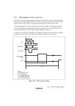
The A/D converter has a built-in sample-and-hold circuit. The A/D converter samples the analog
input at a time t
D
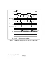
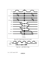
after the ADST bit is set to 1, then starts the conversion. Figure 19-4 shows the
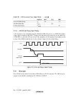
A/D conversion timing. Table 19-4 on the next page indicates the A/D conversion time.
As indicated in figure 19-4 below, the A/D conversion time includes t
D
and the input sampling
time. The length of t
D
varies depending on the timing of the write access to ADCSR. The total
conversion time therefore varies within the ranges indicated in table 19-4.
In scan mode, the values given in table 19-4 are applied to the first conversion. In the second and
subsequent conversions, the conversion time is the same as the first conversion time.
(1)
(2)
CLK
Address bus
Write signal
T
SPL
t
D
t
CONV
Input sampling
timing
ADF
Legend
(1): ADCSR write cycle
(2): ADCSR address
t
D
: Synchronization delay
t
SPL
: Input sampling time
t
CONV
: A/D conversion time
Figure 19.4 A/D Conversion Timing
Содержание HD64465
Страница 25: ...Rev 3 0 03 01 page 6 of 390 ...
Страница 59: ...Rev 3 0 03 01 page 40 of 390 ...
Страница 97: ...Rev 3 0 03 01 page 78 of 390 ...
Страница 147: ...Rev 3 0 03 01 page 128 of 390 ...
Страница 199: ...Rev 3 0 03 01 page 180 of 390 ...
Страница 247: ...Rev 3 0 03 01 page 228 of 390 ...
Страница 385: ...Rev 3 0 03 01 page 366 of 390 ...
Страница 389: ...Rev 3 0 03 01 page 370 of 390 ...
Страница 409: ...Rev 3 0 03 01 page 390 of 390 ...

