Rev. 3.0, 03/01, page 46 of 390
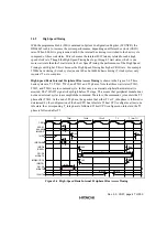
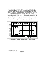
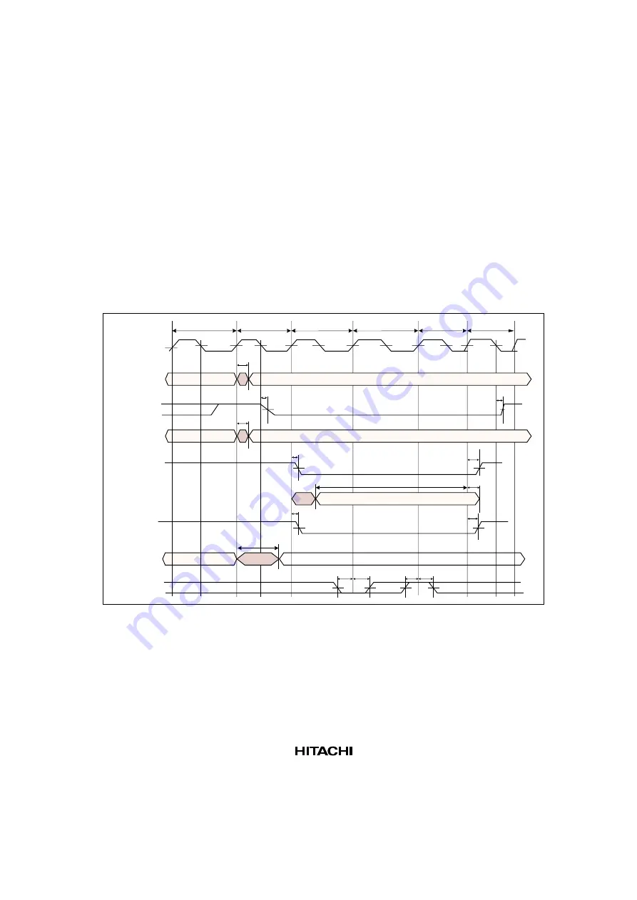
Low-Speed Internal Bus Access Timing with TWe phase is shown in the Figure 5-3. The
diagram shows the cycles are T1, TWs1, TWs2, TWe and T2 phases. Note that there are two wait
states and one external peripheral hardware wait state in command cycle. In this case, the basic
command cycle is not enough for peripheral operation, it is responsible for the peripheral module
to insert its own wait signal before T2 stage. And the *WAIT# signal controlled by the peripheral
module must satisfy the setup/hold time defined in internal peripheral Bus AC timing
specifications. In Figure 5-3, the TWe stands for the external peripheral hardware wait state. The
command cycle can be inserted many TWe states, which depends on the signal *WAIT# of the
peripheral module. At the end of T2 phase, the question that either T1 or T_idle phase is followed
depends on the host CPU bus idle state configuration. If host CPU configures at least one idle state,
the corresponding T_idle phase is followed. If host CPU configures no idle state, the T1 phase is
followed after T2.
T1
T2
TWe
T_idle(T1)
TWs1
t
AD
t
MSD
t
MSD
t
RWD
t
RDD
t
WED
t
WDD
t
WDYS
t
WDYH
t
WDYS
t
WDYH
t
RDD
t
RDH
t
WED
t
RDS
TWs2
CKIO
A20-A1
A24,A25
IMADDR
*
MS#
*
WAIT#
IMRDWR#
IMRD#
(READ)
D31-D0
MODATA
D31-D0
MIDATA
IMWE0/1/2/3#
(WRITE)
Figure 5.3 Low-Speed Internal Peripheral Bus Access Timing With TWe Phase
Содержание HD64465
Страница 25: ...Rev 3 0 03 01 page 6 of 390 ...
Страница 59: ...Rev 3 0 03 01 page 40 of 390 ...
Страница 97: ...Rev 3 0 03 01 page 78 of 390 ...
Страница 147: ...Rev 3 0 03 01 page 128 of 390 ...
Страница 199: ...Rev 3 0 03 01 page 180 of 390 ...
Страница 247: ...Rev 3 0 03 01 page 228 of 390 ...
Страница 385: ...Rev 3 0 03 01 page 366 of 390 ...
Страница 389: ...Rev 3 0 03 01 page 370 of 390 ...
Страница 409: ...Rev 3 0 03 01 page 390 of 390 ...

