Rev. 3.0, 03/01, page 218 of 390
14.3.3
CS4218 or CS4271 TX Controller
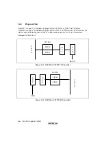
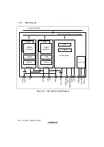
This module, as shown in Fig14-2, contains a TX FIFO, a 32-bit buffer (BUF), a parallel-to-serial
shift register (PSR) and an inferred control circuit. This TX FIFO has two blocks and each block
has 4 32-bit entries. When TX transaction begins, the data stored in TX FIFO will be written to
BUF whenever BUF is empty. The data stored in BUF is written to PSR at specific timing points
of each frame and then the data is serially transmitted to the connected CODEC via serial data
output port. In PIO mode, this module signals an interrupt request to the system under one of the
following conditions: TX FIFO transmit done, underrun and overrun. TX FIFO transmit done
means that any of the two blocks is empty. The system can read SR to realize the source of the
interrupt request and perform related interrupt service routine. In DMA mode, this module signals
a DMA request (DREQ#) whenever TX FIFO is nearly empty, and releases DREQ# whenever TX
FIFO is close to full. DMA mode is more preferred because it will not the increase the CPU
workload.
14.3.4
CS4218 or CS4271 RX Controller
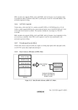
This module, as shown in Fig14-3, contains a RX FIFO, a 32-bit buffer (BUF), a serial-to-parallel
shift register(SPR) and an inferred control circuit. This RX FIFO has two blocks and each block
has 4 32-bit entries. When RX transaction works, serial data from serial data input port is serially
shifted into SPR one bit per serial clock cycle and the data stored in SPR is written to BUF at
specific timing points of each frame. The data stored in BUF is written to RX FIFO whenever BUF
is full. In PIO mode, this module will signal an interrupt request to the system under one of the
following conditions: RX FIFO transmit done, underrun and overrun. RX FIFO transmit done
means that any of the two blocks is full. In DMA mode, this module signals DREQ# whenever RX
FIFO is close to full and releases DREQ# whenever RX FIFO is nearly empty.
14.3.5
AC97 TX Controller
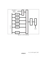
This module, as shown in Fig14-4 on page 169, contains several TX FIFOs, a TX TAG register, a
20-bit buffer, a parallel-to-serial shift register and an inferred control circuit. Each TX FIFO has 4
20-bit entries and is divided into two blocks. The operation mechanism is analogous to CSxx TX
controller. The output of TX TAG register and that of the SLOTREQ register are multiplexed and
selected, depending on which version is selected. If version 2.0 is selected, AC97 RX controller
gets slot request from the receive frame and sends it to AC97 TX controller as the reference of the
valid slot flags of the next transmit frame.
If version 1.03 is selected, AC97 TX controller gets the data in ATAGR register as valid flags of
slots 3-12 of each transmit frame. The valid frame bit of a transmit frame is 0 if all of the valid
flags of slots 1-12 are 0. Otherwise, it is 1. The valid flag of slot1 or 2 of a transmit frame is 1
when CAR or CDR TX FIFO is not empty.
Содержание HD64465
Страница 25: ...Rev 3 0 03 01 page 6 of 390 ...
Страница 59: ...Rev 3 0 03 01 page 40 of 390 ...
Страница 97: ...Rev 3 0 03 01 page 78 of 390 ...
Страница 147: ...Rev 3 0 03 01 page 128 of 390 ...
Страница 199: ...Rev 3 0 03 01 page 180 of 390 ...
Страница 247: ...Rev 3 0 03 01 page 228 of 390 ...
Страница 385: ...Rev 3 0 03 01 page 366 of 390 ...
Страница 389: ...Rev 3 0 03 01 page 370 of 390 ...
Страница 409: ...Rev 3 0 03 01 page 390 of 390 ...

