


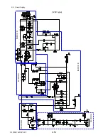
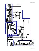


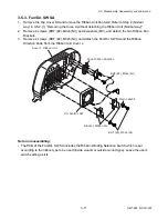

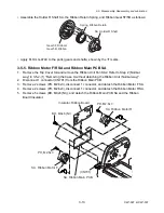

2-5. Power Supply
CLP-621 & CLP-631
2-58
2-5-2. Block A (Noise filter circuit and rush current preventing circuit)
The filter circuit consists of the power switch (SW1) the fuse (F1), the X capacitors (C1, C2), the Y
capacitors (C3, C4), the common mode choke coils (L1 and L2), the varistor (Z1), and the
thermistor (R1).
This circuit eliminates switching noise from the power supply to the main power line. Also, it
eliminates noise from the main power line to the power supply to protect the power supply circuit.
The thermistor R1 suppresses the rush current to the power supply circuit at power on. In
continuous operation, the resistance of R1 is reduced as it is heated, reducing the power loss by
R1.
2-5-3. Block B (Current smoothing circuit)
This block consists of the bridge rectifier DS1, the smoothing capacitors C5-1 and C5-2, and
resistors R8 and R10.
<For 120V type>
Half-wave rectification is performed by the bridge rectifier DS1 and the capacitor C5-1 and also by
the bridge rectifier DS1 and the capacitor C5-2. Thus, the DC voltage across R8 and R9 (output of
this circuit) becomes approx. 2.8-time of the AC input voltage. (It will be approx. 320V DC if the
input voltage is 115V AC.) This DC voltage is supplied to the next converter and driver circuit.
<For 200-240V type>
Full-wave rectification is performed by the bridge rectifier DS1 and the capacitors C5-1 and C5-2.
The DC output of this circuit will be approx. 1.4-time of the AC input voltage. (It will be approx.
320V DC if the input voltage is 230V AC.) This DC voltage is supplied to the next converter and
driver circuit.
The choke coil L3 suppresses high frequency waves to meet the regulations against high
frequency waves.
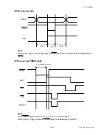
2-5-4. Block C (Converter and driver circuit)
(1) Converter circuit
The converter circuit operates with conducting-angle-controlled reverse method with frequency
fixed. The rectified and smoothed voltage (e.g. 320V DC) is converted by the switching
transformer T1 and then supplied to the secondary circuit.
When Q1 is turned ON, 320V DC is applied to the primary winding N1 of T1. At this time, the
voltage is induced in the secondary windings N3 and N4 and energy is charged in T1 since the
energy flow to the secondary output circuit is blocked by the diodes DS2 and DS3.
When Q1 is turned OFF, the energy polarity is reversed and the energy charged in the
secondary windings N3 and N4 is discharged to the secondary output circuit through DS2 and
DS3. Above operation is repeated and the energy is continuously fed to the secondary output
circuit.
Summary of Contents for CLP-621
Page 1: ...Technical Manual CLP 621 CLP 631 Thermal Transfer Barcode Label Printer JM74961 00F 1 00E 0701...
Page 2: ...CLP 621 CLP 631 ii Copyright 2007 by CITIZEN SYSTEMS JAPAN CO LTD...
Page 4: ...CHAPTER 1 SPECIFICATIONS CLP 621 CLP 631...
Page 13: ...CHAPTER 2 OPERATING PRINCIPLES CLP 621 CLP 631...
Page 73: ...CHAPTER 3 DISASSEMBLY AND MAINTENANCE CLP 621 CLP 631...
Page 126: ...CLP 621 CLP 631 CHAPTER 4 TROUBLESHOOTING...
Page 138: ...CLP 621 CLP 631 CHAPTER 5 PARTS LISTS...
Page 166: ...Chapter 5 Parts Lists CLP 621 CLP 631 5 29 DRAWING NO 7 Control Panel Unit Rev 0 4 3 2 1 5...
Page 177: ...Chapter 5 Parts Lists CLP 621 CLP 631 5 40 DRAWING NO 10 Accessories Rev 0 3 2 4 1...
Page 179: ...CHAPTER 6 CIRCUIT DIAGRAMS CLP 621 CLP 631...
Page 208: ...APPENDICES CLP 621 CLP 631...
Page 212: ...B Mounting Diagrams AP 5 CLP 621 CLP 631 Main PCB Solder side...
Page 214: ...B Mounting Diagrams AP 7 CLP 621 CLP 631 B 3 Ribbon Main PCB Parts side Solder side...
Page 217: ......


