background image

 117

XMEGA B [DATASHEET]

8291B–AVR–01/2013

Note:

Reserved settings will not give any timeout for the window.

Bit 1 – WEN: Window Mode Enable

This bit enables the window mode. In order to change this bit, the WCEN bit in 

“WINCTRL – Window Mode Control 

register” on page 116

 must be written to one at the same time. This bit is protected by the configuration change 

protection mechanism. For a detailed description, refer to 

“Configuration Change Protection” on page 13

.

Bit 0 – WCEN: Window Mode Change Enable

This bit enables the ability to change the configuration of the 

“WINCTRL – Window Mode Control register” on page 116

When writing a new value to this register, this bit must be written to one at the same time for the changes to take effect. 
This bit is protected by the configuration change protection mechanism, but not protected by the WDT lock fuse.

10.7.3 STATUS – Status register

Bit 7:1 – Reserved

These bits are unused and reserved for future use. For compatibility with future devices, always write these bits to zero 
when this register is written.

Bit 0 – SYNCBUSY: Synchronization Busy Flag

This flag is set after writing to the CTRL or WINCTRL registers and the data are being synchronized from the system 
clock to the WDT clock domain. This bit is automatically cleared after the synchronization is finished. Synchronization will 
take place only when the ENABLE bit for the Watchdog Timer is set.

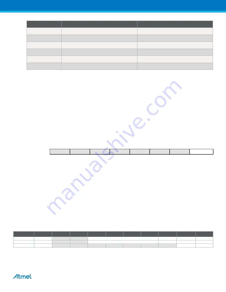
10.8

Register Summary

1010

8KCLK

8.0s

1011

Reserved

1100

Reserved

1101

Reserved

1110

Reserved

1111

Reserved

WPER[3:0]

Group Configuration

Typical Closed Window Periods

Bit

7

6

5

4

3

2

1

0

+0x02

SYNCBUSY

Read/Write R

R

R

R

R

R

R

R

Initial Value 

0

0

0

0

0

0

0

0

Address

Name

Bit 7

Bit 6

Bit 5

Bit 4

Bit 3

Bit 2

Bit 1

Bit 0

Page

+0x00

CTRL

PER[3:0]

ENABLE

CEN

115

+0x01

WINCTRL

WPER[3:0]

WEN

WCEN

116

+0x02

STATUS

SYNCBUSY

117

Summary of Contents for XMEGA B

Page 1: ...Interrupts and programmable multilevel interrupt controller PORT I O ports TC 16 bit timer counters AWeX Advanced waveform extension Hi Res High resolution extension RTC Real time counter USB Univers...

Page 2: ...more detail The register description sections list all registers and describe each register bit and flag with their function This includes details on how to set up and enable various features in the...

Page 3: ...lected devices also have an IEEE std 1149 1 compliant JTAG interface and this can also be used for on chip debug and programming The Atmel AVR XMEGA devices have five software selectable power saving...

Page 4: ...0 7 PB 0 7 JTAG Watchdog Timer Watchdog Oscillator Interrupt Controller DATA BUS Prog Debug Controller VCC GND PORT R 2 PR 0 1 Oscillator Control Real Time Counter Event System Controller JTAG PDI_DA...

Page 5: ...64A QFN VQFN 64M2 BGA 100C1 100C2 QTouch Sense channels 56 56 DMA Controller Channels 2 2 Event System Channels 4 4 QDEC 1 1 Crystal Oscillator 0 4 16MHz XOSC Yes Yes 32 768 kHz TOSC Yes Yes Internal...

Page 6: ...lay Controller LCD Segments 40 25 Common terminals 4 4 Analog to Digital Converter ADC 2 1 Resolution bits 12 12 Sampling speed kbps 300 300 Input channels per ADC 16 8 Conversion channels 1 1 Analog...

Page 7: ...ble to access memories perform calculations control peripherals and execute the program in the flash memory Interrupt handling is described in a separate section Interrupts and Programmable Multilevel...

Page 8: ...two sections the application program section and the boot program section Both sections have dedicated lock bits for write and read write protection The SPM instruction that is used for self programmi...

Page 9: ...ta SRAM can easily be accessed through the five different addressing modes supported in the AVR CPU 3 6 Instruction Execution Timing The AVR CPU is clocked by the CPU clock clkCPU No internal clock di...

Page 10: ...ed before any subroutine calls are executed or before interrupts are enabled During interrupts or subroutine calls the return address is automatically pushed on the stack The return address can be two...

Page 11: ...ter can also be used as an address pointer to read from and or write to the flash program memory signature rows fuses and lock bits Figure 3 5 The X Y and Z registers 7 0 Addr R0 0x00 R1 0x01 R2 0x02...

Page 12: ...gram and data memory space in the device is implemented in the registers 3 10 1 RAMPX RAMPY and RAMPZ Registers The RAMPX RAMPY and RAMPZ registers are concatenated with the X Y and Z registers respec...

Page 13: ...porary registers can also be read and written directly from user software 3 11 1 Accessing 24 and 32 bit Registers For 24 and 32 bit registers the read and write access is done in the same way as desc...

Page 14: ...equest including non maskable interrupts during the CCP period will set the corresponding interrupt flag as normal and the request is kept pending After the CCP period is completed any pending interru...

Page 15: ...enabled CCP 7 2 will always read as zero Table 3 1 shows the signature for the various modes Table 3 1 Modes of CPU change protection 3 14 2 RAMPD Extended Direct Addressing register This register is...

Page 16: ...umber of bits required to address the available data memory is implemented for each device Unused bits will always read as zero 3 14 5 RAMPZ Extended Z Pointer register This register is concatenated w...

Page 17: ...to the top of the stack After reset the stack pointer points to the highest internal SRAM address To prevent corruption when updating the stack pointer from software a write to SPL will automatically...

Page 18: ...o a bit in a register in the register file by the BLD instruction Bit 5 H Half Carry Flag The half carry flag H indicates a half carry in some arithmetic operations Half carry Is useful in BCD arithme...

Page 19: ...Bit 0 Page 0x00 Reserved 0x01 Reserved 0x02 Reserved 0x03 Reserved 0x04 CCP CCP 7 0 15 0x05 Reserved 0x06 Reserved 0x07 Reserved 0x08 RAMPD RAMPD 7 0 15 0x09 RAMPX RAMPX 7 0 16 0x0A RAMPY RAMPY 7 0 16...

Page 20: ...for each microcontroller device type Serial number for each device Calibration bytes for factory calibrated peripherals User signature row One flash page in size Can be read and written from software...

Page 21: ...e the SPM instruction cannot be executed from the application section 4 3 2 Application Table Section The application table section is a part of the application section of the flash memory that can be...

Page 22: ...user parameter storage such as calibration data custom serial number identification numbers random number seeds etc This section is not erased by chip erase commands that erase the flash and requires...

Page 23: ...able through I O memory locations All I O locations can be accessed by the load LD LDS LDD and store ST STS STD instructions which are used to transfer data between the 32 registers in the register fi...

Page 24: ...emory Timing Read and write access to the I O memory takes one CPU clock cycle A write to SRAM takes one cycle and a read from SRAM takes two cycles For burst read DMA new data are available every cyc...

Page 25: ...as normal I O pins 4 13 I O Memory Protection Some features in the device are regarded as critical for safety in some applications Due to this it is possible to lock the I O register related to the c...

Page 26: ...r Byte 2 This register gives the address extended byte when accessing NVM locations 4 14 4 DATA0 Data register 0 The DATA0 DATA1 and DATA registers represent the 24 bit value DATA This holds data duri...

Page 27: ...for programming commands 4 14 8 CTRLA Control register A Bit 7 1 Reserved These bits are unused and reserved for future use For compatibility with future devices always write these bits to zero when...

Page 28: ...on page 14 for details on the CCP 4 14 10 INTCTRL Interrupt Control register Bit 7 4 Reserved These bits are unused and reserved for future use For compatibility with future devices always write thes...

Page 29: ...ts are unused and reserved for future use For compatibility with future devices always write these bits to zero when this register is written Bit 1 EELOAD EEPROM Page Buffer Active Loading The EELOAD...

Page 30: ...f the closed window for the Watchdog Timer in Window Mode During reset these fuse bits are automatically written to the WPER bits Watchdog Window Mode Control Register refer to WINCTRL Window Mode Con...

Page 31: ...fuse Note 1 See the device datasheet for alternate TOSC position Bit 4 2 Reserved These fuse bits are reserved For compatibility with future devices always write these bits to one when this register...

Page 32: ...be programmed to lock the watchdog timer configuration When this fuse is programmed the watchdog timer configuration cannot be changed and the ENABLE bit in the watchdog CTRL register is automatically...

Page 33: ...EEPROM is used to store data independently of the software revision Table 4 8 EEPROM preserved through chip erase Changes to the EESAVE fuse bit take effect immediately after the write timeout elapses...

Page 34: ...from the application section is not allowed to read from the boot loader section If the interrupt vectors are placed in the application section interrupts are disabled while executing from the boot lo...

Page 35: ...No lock no restrictions for SPM and E LPM accessing the application table section 10 WLOCK Write lock SPM is not allowed to write the application table 01 RLOCK Read lock E LPM executing from the boo...

Page 36: ...7 0 RCOSC32K 7 0 Internal 32 768kHz Oscillator Calibration Value This byte contains the oscillator calibration value for the internal 32 768kHz oscillator Calibration of the oscillator is performed du...

Page 37: ...ther with the wafer number and wafer coordinates this gives a serial number for the device Bit 7 0 LOTNUM0 7 0 Lot Number Byte 0 This byte contains byte 0 of the lot number for the device 4 16 7 LOTNU...

Page 38: ...lot number for the device 4 16 12 WAFNUM Wafer Number register Bit 7 0 WAFNUM 7 0 Wafer Number This byte contains the wafer number for each device Together with the lot number and wafer coordinates t...

Page 39: ...ate X for the device 4 16 15 COORDY0 Wafer Coordinate Y register 0 Bit 7 0 COORDY0 7 0 Wafer Coordinate Y Byte 0 This byte contains byte 0 of wafer coordinate Y for the device 4 16 16 COORDY1 Wafer Co...

Page 40: ...ator When this calibration value is written to calibration register B for the 32MHz DFLL the oscillator is calibrated to 48MHz to enable full speed USB operation from internal oscillator Note The COMP...

Page 41: ...DCBCAL0 7 0 ADCB Calibration Byte 1 This byte contains byte 1 of the ADCB calibration data and must be loaded into the ADCB CALH register 4 16 24 TEMPSENSE0 Temperature Sensor Calibration register 0 T...

Page 42: ...t identifies each microcontroller device type For details on the actual ID refer to the device datasheet Bit 7 0 DEVID0 7 0 Device ID Byte 0 Byte 0 of the device ID This byte will always be read as 0x...

Page 43: ...CUCR MCU Control register Bit 7 1 Reserved These bits are unused and reserved for future use For compatibility with future devices always write these bits to zero when this register is written Bit 0 J...

Page 44: ...Analog start up delay 4 18 8 EVSYSLOCK Event System Lock register Bit 7 1 Reserved These bits are unused and reserved for future use For compatibility with future devices always write these bits to ze...

Page 45: ...o when this register is written Bit 0 AWEXCLOCK Advanced Waveform Extension Lock for TCC0 Setting this bit will lock all registers in the AWEXC module for Timer Counter C0 foragainst further modificat...

Page 46: ...x09 Reserved 0x0A CMD CMD 6 0 26 0x0B CTRLA CMDEX 27 0x0C CTRLB EEMAPEN FPRM EPRM SPMLOCK 27 0x0D INTCTRL SPMLVL 1 0 EELVL 1 0 28 0x0E Reserved 0x0F STATUS NVMBUSY FBUSY EELOAD FLOAD 28 0x10 LOCKBITS...

Page 47: ...OORDX0 7 0 39 0x13 NO COORDX1 COORDX1 7 0 39 0x14 NO COORDY0 COORDY0 7 0 39 0x15 NO COORDY1 COORDY1 7 0 39 0x16 Reserved 0x17 Reserved 0x18 Reserved 0x19 Reserved 0x1A USBCAL0 USBCAL0 7 0 40 0x1B USBC...

Page 48: ...0x09 Reserved 0x0A Reserved 0x0B Reserved 0x0C Reserved 0x0D Reserved 0x0E Reserved 0x0F Reserved Address Name Bit 7 Bit 6 Bit 5 Bit 4 Bit 3 Bit 2 Bit 1 Bit 0 Page 0x00 DEVID0 DEVID0 7 0 42 0x01 DEVI...

Page 49: ...ers The DMA controller can move data between SRAM and peripherals between SRAM locations and directly between peripheral registers With access to all peripherals the DMA controller can handle automati...

Page 50: ...urst Transfer Since the AVR CPU and DMA controller use the same data buses a block transfer is divided into smaller burst transfers The burst transfer is selectable to 1 2 4 or 8 bytes This means that...

Page 51: ...and destination addresses are stored by the DMA controller and so the source and destination addresses can be individually configured to be reloaded at the following points End of each burst transfer...

Page 52: ...el are cleared A software reset can be done only when the DMA channel is disabled 5 11 Protection In order to ensure safe operation some of the channel registers are protected during a transaction Whe...

Page 53: ...ble Buffer Mode This bit enables the double buffer mode Bit 1 Reserved This bit is unused and reserved for future use For compatibility with future devices always write this bits to zero when this reg...

Page 54: ...channel is disabled when the channel n transaction complete interrupt flag is set or if the DMA channel n error interrupt flag is set Bit 3 2 Reserved These bits are unused and reserved for future use...

Page 55: ...g a one to this bit will be ignored as long as the channel is enabled CHEN 1 This bit is automatically cleared when reset is completed Bit 5 REPEAT Repeat Mode Setting this bit enables the repeat mode...

Page 56: ...is set or when the channel error interrupt flag is set BURSTLEN 1 0 Group Configuration Description 00 1BYTE 1 byte burst mode 01 2BYTE 2 bytes burst mode 10 4BYTE 4 bytes burst mode 11 8BYTE 8 bytes...

Page 57: ...3 2 ERRINTLVL 1 0 Channel Error Interrupt Level These bits enable the interrupt for DMA channel transfer errors and select the interrupt level as described in Interrupts and Programmable Multilevel I...

Page 58: ...he DMA channel destination address mode according to Table 5 7 These bits cannot be changed if the channel is busy Table 5 7 DMA channel destination address mode settings SRCDIR 1 0 Group Configuratio...

Page 59: ...t will be lost Since a DMA request can clear the interrupt flag interrupts can be lost Note For most trigger sources the request is cleared by accessing a register belonging to the peripheral with the...

Page 60: ...of this register is 0x1 If a user writes 0x0 to this register and fires a DMA trigger DMA will be doing 0xFFFF transfers Table 5 9 DMA trigger source offset values for event system triggers TRGSRC Off...

Page 61: ...lock transfer if the DMA has to serve a limited number of repeated block transfers When repeat mode is enabled the channel is disabled when REPCNT reaches zero and the last block transfer is completed...

Page 62: ...TADDR2 represent the 24 bit value DESTADDR which is the DMA channel destination address DESTADDR2 holds the most significant byte in the register DESTADDR may be automatically incremented or decrement...

Page 63: ...and writing 24 bit values require special attention For details refer to Accessing 24 and 32 bit Registers on page 13 Bit 7 0 DESTADDR 23 16 Channel Destination Address byte 2 These bits hold byte 2 o...

Page 64: ...0 Reserved Address Name Bit 7 Bit 6 Bit 5 Bit 4 Bit 3 Bit 2 Bit 1 Bit 0 Page 0x00 CTRLA ENABLE RESET REPEAT TRFREQ SINGLE BURSTLEN 1 0 55 0x01 CTRLB CHBUSY CHPEND ERRIF TRNIF ERRINTLVL 1 0 TRNINTLVL 1...

Page 65: ...ort and predictable response times between peripherals It allows for autonomous peripheral control and interaction without the use of interrupts CPU or DMA controller resources and is thus a powerful...

Page 66: ...state within a peripheral has occurred is called an event There are two main types of events signaling events and data events Signaling events only indicate a change of state while data events contai...

Page 67: ...l Clock Events Each event channel includes a peripheral clock prescaler with a range from 1 no prescaling to 32768 This enables configurable periodic event generation based on the peripheral clock It...

Page 68: ...ce to any event users The output from a multiplexer is referred to as an event channel For each peripheral it is selectable if and how incoming events should trigger event actions Details on configura...

Page 69: ...all devices 6 5 Event Timing An event normally lasts for one peripheral clock cycle but some event sources such as a low level on an I O pin will generate events continuously Details on this are desc...

Page 70: ...decoded and how they can be generated The QDEC and related features control and status registers are available for event channel 0 Table 6 2 Quadrature decoder data events 6 7 1 Quadrature Operation...

Page 71: ...al 1 Set up a QDEC index QINDX 2 Select a third pin for QINDX input 3 Set the pin direction for QINDX as input 4 Set the pin configuration for QINDX to sense both edges 5 Select QINDX as a multiplexer...

Page 72: ...ero Table 6 3 CHnMUX 7 0 bit settings Bit 7 6 5 4 3 2 1 0 CHnMUX 7 0 Read Write R W R W R W R W R W R W R W R W Initial Value 0 0 0 0 0 0 0 0 CHnMUX 7 4 CHnMUX 3 0 Group Configuration Event Source 000...

Page 73: ...o 15 1001 X X X X Reserved 1010 X X X X Reserved 1011 X X X X Reserved 1100 0 E See Table 6 4 Timer counter C0 event type E 1100 1 E See Table 6 4 Timer counter C1 event type E 1101 0 E See Table 6 4...

Page 74: ...et the event channel will be used as a QDEC index source and the index data event will be enabled This bit is available only for CH0CTRL and CH2CTRL Bit 3 QDEN Quadrature Decode Enable Setting this bi...

Page 75: ...ly generating a data event This register must be written before the STROBE register For details See STROBE Strobe register on page 75 011 4SAMPLES Four samples 100 5SAMPLES Five samples 101 6SAMPLES S...

Page 76: ...0 72 0x02 CH2MUX CH2MUX 7 0 72 0x03 CH3MUX CH3MUX 7 0 72 0x04 Reserved 0x05 Reserved 0x06 Reserved 0x07 Reserved 0x08 CH0CTRL QDIRM 1 0 QDIEN QDEN DIGFILT 2 0 74 0x09 CH1CTRL DIGFILT 2 0 74 0x0A CH2C...

Page 77: ...rnal oscillators and external crystal oscillator and resonator support A high frequency phase locked loop PLL and clock prescalers can be used to generate a wide range of clock frequencies A calibrati...

Page 78: ...e Memory Watchdog Timer Brown out Detector System Clock Prescalers USB Prescaler System Clock Multiplexer SCLKSEL PLLSRC DIV32 32 kHz Int ULP 32 768 kHz Int OSC 32 768 kHz TOSC 2 MHz Int Osc 32 MHz In...

Page 79: ...ck It has a separate clock source selection in order to avoid system clock source limitations when USB is used 7 4 Clock Sources The clock sources are divided in two main groups internal oscillators a...

Page 80: ...automatic run time calibration of the oscillator to compensate for temperature and voltage drift and optimize the oscillator accuracy 7 4 2 External Clock Sources The XTAL1 and XTAL2 pins can be used...

Page 81: ...escaler block that can divide the clock signal by a factor from 1 to 2048 before it is routed to the CPU and peripherals The prescaler settings can be changed from software during normal operation The...

Page 82: ...on cannot be changed when the PLL is in use The PLL must be disabled before a new configuration can be written It is not possible to use the PLL before the selected clock source is stable and the PLL...

Page 83: ...nature row and written to the 32MHz CAL register before the DFLL is enabled with USB SOF as reference source The value that should be written to the COMP register is given by the following formula Whe...

Page 84: ...oscillator control register and system clock selection register to their default values Set the failure detection interrupt flag for the failing clock source PLL or external clock Issue a non maskable...

Page 85: ...s not stable The old clock can not be disabled until the clock switching is completed Table 7 1 System clock selection 7 9 2 PSCTRL Prescaler Control register This register is protected by the configu...

Page 86: ...R4 clock Prescaler C will set the clock frequency for the ClkPER and ClkCPU clocks relative to the ClkPER2 clock Refer to Figure 7 5 on page 81 fore more details Table 7 3 Prescaler B and C division f...

Page 87: ...mpatibility with future devices always write these bits to zero when this register is written Bit 3 1 RTCSRC 2 0 RTC and LCD Clock Source These bits select the clock source for the Real Time Counter R...

Page 88: ...Bit 2 1 USBSRC 1 0 USB Clock Source These bits select the clock source for the USB module according to Table 7 6 Table 7 6 USB clock source Note 1 The 32MHz internal oscillator must be calibrated to...

Page 89: ...e source for the system clock See STATUS Status register on page 89 Bit 0 RC2MEN 2MHz Internal Oscillator Enable Setting this bit enables the 2MHz internal oscillator The oscillator must be stable bef...

Page 90: ...llator and increase the swing on the XTAL2 pin This allows for driving crystals with higher load or higher frequency than specified by the FRQRANGE bits This function is enabled if the 0 4 16MHz Cryst...

Page 91: ...tection A non maskable interrupt will be issued when PLLFDIF is set This bit is protected by the configuration change protection mechanism Refer to Configuration Change Protection on page 14 for detai...

Page 92: ...o be used as the source clock Bit 5 PLLDIV PLL Divided Output Enable Setting this bit will divide the output from the PLL by 2 Bit 4 0 PLLFAC 4 0 Multiplication Factor These bits select the multiplica...

Page 93: ...e unused and reserved for future use For compatibility with future devices always write these bits to zero when this register is written Bit 0 ENABLE Enable Setting this bit enables the DFLL and auto...

Page 94: ...e unused and reserved for future use For compatibility with future devices always write these bits to zero when this register is written Bit 5 0 CALB 5 0 DFLL Calibration bits These bits hold the part...

Page 95: ...pare register byte 2 Bit 7 0 COMP2 15 8 Compare Register Byte 2 These bits hold byte 2 of the 16 bit compare register Table 7 11 Nominal DFLL32M COMP values for different output frequencies Bit 7 6 5...

Page 96: ...it 3 Bit 2 Bit 1 Bit 0 Page 0x00 CTRL PLLEN XOSCEN RC32KEN R32MEN RC2MEN 89 0x01 STATUS PLLRDY XOSCRDY RC32KRD R32MRDY RC2MRDY 89 0x02 XOSCCTRL FRQRANGE 1 0 X32KLPM XOSCPW XOSCSEL 3 0 90 XOSCSEL 0x03...

Page 97: ...ate of the peripheral is frozen and there is no power consumption from that peripheral This reduces the power consumption in active mode and idle sleep modes and enables much more fine tuned power man...

Page 98: ...re stopped This allows operation only of asynchronous modules that do not require a running clock The only interrupts that can wake up the MCU are the two wire interface address match interrupt asynch...

Page 99: ...bled if not used In other sleep modes the ADC is automatically disabled When the ADC is turned off and on again the next conversion will be an extended conversion Refer to ADC Analog to Digital Conver...

Page 100: ...chip Debug Systems If the On chip debug system is enabled and the chip enters sleep mode the main clock source is enabled and hence always consumes power In the deeper sleep modes this will contribut...

Page 101: ...ed to write SEN just before executing the SLEEP instruction and clear it immediately after waking up 8 7 Register Description Power Reduction 8 7 1 PRGEN General Power Reduction register Bit 7 LCD LCD...

Page 102: ...s before it was stopped Bit 0 DMA DMA Controller Setting this bit stops the clock to the DMA controller This bit can be set only if the DMA controller is disabled 8 7 2 PRPA B Power Reduction Port A B...

Page 103: ...operation Bit 3 SPI Serial Peripheral Interface Setting this bit stops the clock to the SPI When this bit is cleared the peripheral should be reinitialized to ensure proper operation Bit 2 HIRES High...

Page 104: ...me Bit 7 Bit 6 Bit 5 Bit 4 Bit 3 Bit 2 Bit 1 Bit 0 Page 0x00 CTRL SMODE 2 0 SEN 101 Address Name Bit 7 Bit 6 Bit 5 Bit 4 Bit 3 Bit 2 Bit 1 Bit 0 Page 0x00 PRGEN LCD USB AES RTC EVSYS DMA 101 0x01 PRPA...

Page 105: ...re immediately tri stated The program counter is set to the reset vector location and all I O registers are set to their initial values The SRAM content is kept However if the device accesses the SRAM...

Page 106: ...m when all reset requests are released The reset delay is timed from the 1kHz output of the ultra low power ULP internal oscillator and in addition 24 System clock clkSYS cycles are counted before res...

Page 107: ...ed to power down the device properly when the VCC falls and drops below the VPOT level The VPOT level is higher for falling VCCthan for rising VCC Consult the datasheet for POR characteristics data Fi...

Page 108: ...are nominal values only For accurate actual numbers consult the device datasheet 2 Changing these fuse bits will have no effect until leaving programming mode The BOD circuit has three modes of opera...

Page 109: ...eset circuit is connected to the external RESET pin The external reset will trigger when the RESET pin is driven below the RESET pin threshold voltage VRST for longer than the minimum pulse period tEX...

Page 110: ...ster The reset will be issued within two CPU clock cycles after writing the bit It is not possible to execute any instruction from when a software reset is requested until it is issued Figure 9 7 Soft...

Page 111: ...r on reset or by writing a one to the bit location Bit 2 BORF Brownout Reset Flag This flag is set if a brownout reset occurs The flag will be cleared by a power on reset or by writing a one to the bi...

Page 112: ...en a reset is issued This bit is protected by the configuration change protection mechanism For details refer to Configuration Change Protection on page 13 9 6 Register Summary Address Name Bit 7 Bit...

Page 113: ...eset If the WDT is reset outside this window either too early or too late a system reset will be issued Compared to the normal mode this can also catch situations where a code error causes constant WD...

Page 114: ...llator Due to the ultra low power design the oscillator is not very accurate and so the exact timeout period may vary from device to device When designing software which uses the WDT this device to de...

Page 115: ...eriod WDP fuses which are loaded at power on In order to change these bits the CEN bit must be written to 1 at the same time These bits are protected by the configuration change protection mechanism F...

Page 116: ...For compatibility with future devices always write these bits to zero when this register is written Bit 5 2 WPER 3 0 Window Mode Timeout Period These bits determine the closed window period as a numbe...

Page 117: ...not protected by the WDT lock fuse 10 7 3 STATUS Status register Bit 7 1 Reserved These bits are unused and reserved for future use For compatibility with future devices always write these bits to ze...

Page 118: ...st interrupt vector address has the highest interrupt priority Low level interrupts have an optional round robin scheduling scheme to ensure that all interrupts are serviced within a certain amount of...

Page 119: ...flag will be set and remembered until global interrupts are enabled All pending interrupts are then executed according to their order of priority Interrupts can be blocked when executing code from a...

Page 120: ...instruction If an interrupt occurs when the device is in sleep mode the interrupt execution response time is increased by five clock cycles In addition the response time is increased by the start up t...

Page 121: ...h interrupts are acknowledged is decided both by the level and the priority of the interrupt request Interrupts can be organized in a static or dynamic round robin priority scheme High and medium leve...

Page 122: ...tatic priority where some interrupts might never be served the PMIC offers round robin scheduling for low level interrupts When round robin scheduling is enabled the interrupt vector address for the l...

Page 123: ...rs are not used and regular program code can be placed at these locations This is also the case if the Reset Vector is in the Application section while the Interrupt Vectors are in the Boot section or...

Page 124: ...when returning RETI from the interrupt handler Bit 0 LOLVLEX Low level Interrupt Executing This flag is set when a low level interrupt is executing or when the interrupt handler has been interrupted b...

Page 125: ...uture use For compatibility with future devices always write these bits to zero when this register is written Bit 2 HILVLEN High level Interrupt Enable 1 When this bit is set all high level interrupts...

Page 126: ...of up to eight port pins pin 0 to 7 Each port pin can be configured as input or output with configurable driver and pull settings They also implement synchronous and asynchronous input sensing with in...

Page 127: ...ro pin n is driven low The IN register is used for reading pin values A pin value can always be read regardless of whether the pin is configured as input or output except if digital input is disabled...

Page 128: ...simplified schematics in Figure 12 2 on page 128 to Figure 12 7 on page 130 12 3 1 Totem pole In the totem pole push pull configuration the pin is driven low or high according to the corresponding bi...

Page 129: ...2 Bus keeper In the bus keeper configuration it provides a weak bus keeper that will keep the pin at its logic level when the pin is no longer driven to high or low If the last level on the pin bus wa...

Page 130: ...is used this is also active if the pin is set as input Figure 12 6 Output configuration Wired OR with optional pull down 12 3 4 Wired AND In the wired AND configuration the pin will be driven low when...

Page 131: ...e pin value cannot be read The IN register bit and the preceding flip flop constitute a synchronizer The synchronizer introduces a delay on the internal signal line Figure 12 8 on page 131 shows a tim...

Page 132: ...r asynchronous sensing only port pin 2 on each port has full asynchronous sense support This means that for edge detection pin 2 will detect and latch any edge and it will always trigger an interrupt...

Page 133: ...be generated on a low level the pin configuration must be set to inverted I O Table 12 4 Event sense support Sense Settings Supported Interrupt Description Rising edge Yes Always triggered Falling edg...

Page 134: ...tion for that peripheral The port override signals and related logic grey are shown in Figure 12 10 on page 134 These signals are not accessible from software but are internal signals between the over...

Page 135: ...rite operation to only one of the port pin configuration registers A mask register decides which port pin is configured when one port pin register is written while avoiding several pins being written...

Page 136: ...the corresponding bit in the DIR register Reading this register will return the value of the DIR register 12 12 3 DIRCLR Data Direction Clear register Bit 7 0 DIRCLR 7 0 Port Data Direction Clear This...

Page 137: ...n be used instead of a read modify write to set the output value of individual pins to one Writing a one to a bit will set the corresponding bit in the OUT register Reading this register will return t...

Page 138: ...s not sampled and cannot be read if the digital input buffers are disabled 12 12 10INTCTRL Interrupt Control register Bit 7 4 Reserved These bits are unused and reserved for future use For compatibili...

Page 139: ...he PINnCTRL registers 12 12 13INTFLAGS Interrupt Flag register Bit 7 2 Reserved These bits are unused and reserved for future use For compatibility with future devices always write these bits to zero...

Page 140: ...l move the location of OC0D from Px3 to Px7 Bit 2 TC0C Timer Counter 0 Output Compare C Setting this bit will move the location of OC0C from Px2 to Px6 Bit 1 TC0B Timer Counter 0 Output Compare B Sett...

Page 141: ...n page 141 The sense configuration decides how the pin can trigger port interrupts and events If the input buffer is not disabled the input cannot be read in the IN register Table 12 6 Input sense con...

Page 142: ...nuously generate events 2 Only PORTA PORTF support the input buffer disable option If the pin is used for analog functionality such as AC or ADC it is recommended to configure the pin to INPUT_DISABLE...

Page 143: ...s equal to accessing the actual port registers See Table 12 7 on page 144 for configuration Bit 3 0 VP0MAP Virtual Port 0 Mapping These bits decide which ports should be mapped to Virtual Port 0 The r...

Page 144: ...used and the CLKOUT bits must be set differently from those of EVOUT The port pin must be configured as output for the event to be available on the pin VPnMAP 3 0 Group Configuration Description 0000...

Page 145: ...The port pin must be configured as output for the clock to be available on the pin Table 12 10 shows the possible configurations Table 12 8 Event output pin selection EVOUT 1 0 Group Configuration Des...

Page 146: ...em is output to the port pin Table 12 11 shows the available selections Bit 7 6 5 4 3 2 1 0 0x06 EVOUTSEL 2 0 Read Write R R R R R R W R W R W Initial Value 0 0 0 0 0 0 0 0 Table 12 11 Event channel o...

Page 147: ...ntrol register B When a port is mapped as virtual accessing this register is identical to accessing the actual OUT register for the port 12 14 3 IN Data Input Value register Bit 7 0 IN 7 0 Data Input...

Page 148: ...tion and the pin is set as source for port interrupt n Writing a one to this flag s bit location will clear the flag For enabling and executing the interrupt refer to the interrupt level description T...

Page 149: ...0 ISC 2 0 141 0x11 PIN1CTRL INVEN OPC 2 0 ISC 2 0 141 0x12 PIN2CTRL INVEN OPC 2 0 ISC 2 0 141 0x13 PIN3CTRL INVEN OPC 2 0 ISC 2 0 141 0x14 PIN4CTRL INVEN OPC 2 0 ISC 2 0 141 0x15 PIN5CTRL INVEN OPC 2...

Page 150: ...0 XMEGA B DATASHEET 8291B AVR 01 2013 12 18 Interrupt Vector Summary Ports Offset Source Interrupt Description 0x00 INT0_vect Port interrupt vector 0 offset 0x02 INT1_vect Port interrupt vector 1 offs...

Page 151: ...bit timer counters TC Their capabilities include accurate program execution timing frequency and waveform generation and input capture with time and frequency measurement of digital signals Two timer...

Page 152: ...timer counter and closely related peripherals 13 2 1 Definitions The following definitions are used throughout the documentation Table 13 1 Timer counter definitions In general the term timer is used...

Page 153: ...also compared to the CCx registers These comparisons can be used to generate interrupt requests request DMA transactions or generate events for the event system The waveform generator modes use these...

Page 154: ...vent system The event selection EVSEL and event action EVACT settings are used to trigger an event action from one or more events This is referred to as event action controlled operation of the counte...

Page 155: ...ring Both the CCx and CCxBUF registers are available as an I O register This allows initialization and bypassing of the buffer register and the double buffering function 13 6 Counter Operation Dependi...

Page 156: ...ll be used to select between up 1 and down 0 The pin configuration must be set to low level sensing Event system controlled quadrature decode counting 13 6 3 32 bit Operation Two timer counters can be...

Page 157: ...ure channels to capture external events and give them a timestamp To use capture the counter must be set for normal operation Events are used to trigger the capture i e any events from the event syste...

Page 158: ...he input capture event action makes the enabled capture channel perform an input capture on an event The interrupt flags will be set and indicate that there is a valid capture result in the correspond...

Page 159: ...ting the pulse width measure event action makes the enabled compare channel perform the input capture action on falling edge events and the restart action on rising edge events The counter will then r...

Page 160: ...h The match will set the CC channel s interrupt flag at the next timer clock cycle and the event and optional interrupt are generated The compare buffer register provides double buffer capability equi...

Page 161: ...ure 13 15 shows how the counter counts from BOTTOM to TOP and then restarts from BOTTOM The waveform generator WG output is set on the compare match between the CNT and CCx registers and cleared at TO...

Page 162: ...e period register PER defines the PWM resolution The minimum resolution is 2 bits PER 0x0003 and the maximum resolution is 16 bits PER MAX The following equation calculate the exact resolution for dua...

Page 163: ...timer counter and the DMA action that will clear the transfer trigger For more details on using DMA refer to DMAC Direct Memory Access Controller on page 49 Table 13 2 DMA request sources 13 11 Timer...

Page 164: ...g these bits in the FRQ or PWM waveform generation mode of operation will override the port output register for the corresponding OCn output pin When input capture operation is selected the CCxEN bits...

Page 165: ...Timer waveform generation mode 13 12 3 CTRLC Control register C Bit 7 4 Reserved These bits are unused and reserved for future use For compatibility with future devices always write these bits to zero...

Page 166: ...for the carry propagation delay when cascading two counters via the event system Bit 3 0 EVSEL 3 0 Timer Event Source Select These bits select the event channel source for the timer counter For the s...

Page 167: ...ices always write these bits to zero when this register is written 0100 Reserved 0101 Reserved 0110 Reserved 0111 Reserved 1nnn CHn Event channel n n 0 7 EVSEL 3 0 Group Configuration Event Source Bit...

Page 168: ...g CTRLxCLR and one for setting the register bits CTRLxSET when written Both memory locations will give the same result when read The individual status bit can be set by writing a one to its bit locati...

Page 169: ...on page 168 for information on how to access this type of status register Bit 7 5 Reserved These bits are unused and reserved for future use For compatibility with future devices always write these b...

Page 170: ...ways write these bits to zero when this register is written Bit 1 ERRIF Error Interrupt Flag This flag is set on multiple occasions depending on the mode of operation In the FRQ or PWM waveform genera...

Page 171: ...16 bit Registers on page 13 Bit 7 0 CNT 7 0 Counter low byte These bits hold the LSB of the 16 bit counter register 13 12 13CNTH Counter register High Bit 7 0 CNT 15 8 Counter high byte These bits ho...

Page 172: ...ts form the comparators are then used for generating waveforms CCx registers are updated with the buffer value from their corresponding CCxBUF register when an UPDATE condition occurs Bit 7 0 CCx 7 0...

Page 173: ...0CCxBUFL Compare or Capture x Buffer register Low The CCxBUFH and CCxBUFL register pair represents the 16 bit value CCxBUF These 16 bit registers serve as the buffer for the associated compare or capt...

Page 174: ...Capture x Buffer register High Bit 7 0 CCxBUF 15 8 Compare or Capture Buffer high byte These bits hold the MSB of the 16 bit compare or capture buffer register Bit 7 6 5 4 3 2 1 0 CCxBUF 15 8 Read Wr...

Page 175: ...1 CNTH CNT 15 8 171 0x22 to Reserved 0x26 PERL PER 7 0 171 0x27 PERH PER 8 15 172 0x28 CCAL CCA 7 0 172 0x29 CCAH CCA 15 8 172 0x2A CCBL CCB 7 0 172 0x2B CCBH CCB 15 8 172 0x2C CCCL CCC 7 0 172 0x02D...

Page 176: ...dth modulation PWM channels with individually controlled duty cycles and is intended for applications that require a high number of PWM channels The two eight bit timer counters in this system are ref...

Page 177: ...nd event selection Figure 14 2 Clock selection Base Counter Compare Unit x A B C D Counter HPER 0 Control Logic CTRLA HUNF INT DMA Req BOTTOML LPER Compare Unit x A B C D Waveform Generation LCMPx INT...

Page 178: ...ounter operation As shown in Figure 14 3 the counter can change the counter value while running The write access has higher priority than the count clear and reloads and will be immediate 14 5 1 Chang...

Page 179: ...ution The minimum resolution is two bits PER 0x0003 and the maximum resolution is eight bits PER MAX The following equation is used to calculate the exact resolution for a single slope PWM RPWM_SS wav...

Page 180: ...g request is listed in Table 14 1 Table 14 1 DMA request sources 14 9 Timer Counter Commands A set of commands can be given to the timer counter by software to immediately change the state of the modu...

Page 181: ...e Compare Enable x Setting these bits will enable the compare output and override the port output register for the corresponding OCn output pin Bit 7 6 5 4 3 2 1 0 0x00 CLKSEL 3 0 Read Write R R R R R...

Page 182: ...en this register is written Bit 0 1 BYTEM 1 0 Byte Mode These bits select the timer counter operation mode according to Table 14 3 Table 14 3 Byte mode Bit 7 6 5 4 3 2 1 0 0x02 HCMPD HCMPC HCMPB HCMPA...

Page 183: ...register B Bit 7 0 LCMPxINTLVL 1 0 Low byte Compare x Interrupt Level These bits enable the low byte timer compare interrupt and select the interrupt level as described in Interrupts and Programmable...

Page 184: ...e these bits to zero when this register is written Bit 1 HUNFIF High byte Timer Underflow Interrupt Flag HUNFIF is set on a BOTTOM underflow condition This flag is automatically cleared when the corre...

Page 185: ...0 11LPER Low byte Period register Bit 7 0 LPER 7 0 LPER contains the eight bit period value for the low byte timer counter 14 10 12HPER High byte Period register Bit 7 0 HPER 7 0 HPER contains the eig...

Page 186: ...ating waveforms 14 10 14HCMPx High byte Compare register x Bit 7 0 HCMPx 7 0 x A B C D HCMPx contains the eight bit compare value for the high byte timer counter These registers are all continuously c...

Page 187: ...gister 185 0x22 to Reserved 0x26 LPER Low byte Timer Counter Period Register 185 0x27 HPER High byte Timer Counter Period Register 186 0x28 LCMPA Low byte Compare Register A 186 0x29 HCMPA High byte C...

Page 188: ...marily intended for use with different types of motor control and other power control applications It enables low and high side output with dead time insertion and fault protection for disabling and s...

Page 189: ...he DTI unit is bypassed The fault protection unit is connected to the event system enabling any event to trigger a fault condition that will disable the AWeX output The event system ensures predictabl...

Page 190: ...re channel in timer counter 0 Figure 15 3 on page 191 shows the block diagram of one DTI generator The four channels have a common register that controls the OUT0 OUTOVEN0 CCAEN DTICCAEN INVEN0 OUT1 O...

Page 191: ...ad of DTHS register Figure 15 4 Dead time generator timing diagram 15 5 Pattern Generation The pattern generator unit reuses the DTI registers to produce a synchronized bit pattern across the port it...

Page 192: ...fault is detected the direction clear action will clear the direction DIR register in the associated port setting all port pins as tri stated inputs The fault detection flag is set the timer counter...

Page 193: ...anged To avoid unintentional changes in the fault event setup it is possible to lock the event system channel configuration by writing the corresponding event system lock register For more details ref...

Page 194: ...Bit 3 0 DTICCxEN Dead Time Insertion CCx Enable Setting these bits enables the dead time generator for the corresponding CC channel This will override the timer counter waveform outputs 15 7 2 FDEMAS...

Page 195: ...ycle by cycle mode is used In latched mode the waveform output will remain in the fault state until the fault condition is no longer active and the FDF has been cleared by software When both condition...

Page 196: ...set the corresponding DT buffer is written and contains valid data that will be copied into the DTHS register on the next UPDATE condition If this bit is zero no action will be taken The connected ti...

Page 197: ...ister is copied to the DTLS register on an UPDATE condition 15 7 10 DTHSBUF Dead time High Side Buffer register Bit 7 0 DTHSBUF Dead time High Side Buffer This register is the buffer for the DTHS regi...

Page 198: ...t 7 6 5 4 3 2 1 0 0x0C OUTOVEN 7 0 Read Write R W 1 R W 1 R W 1 R W 1 R W 1 R W 1 R W 1 R W 1 Initial Value 0 0 0 0 0 0 0 0 Address Name Bit 7 Bit 6 Bit 5 Bit 4 Bit 3 Bit 2 Bit 1 Bit 0 Pag 0x00 CTRL P...

Page 199: ...ignore its two least significant bits lsb in the counter and counts by four for each peripheral clock cycle Overflow underflow and compare match of the 14 most significant bits msb is done in the time...

Page 200: ...EN 1 0 High Resolution Enable These bits enables the high resolution mode for a timer counter according to Table 16 1 Setting one or both HREN bits will enable high resolution waveform generation outp...

Page 201: ...n The faster 32 768kHz output can be selected if the RTC needs a resolution higher than 1ms The RTC can also be clocked from an external clock signal the 32 768kHz internal oscillator or the 32kHz int...

Page 202: ...for the RTC 17 2 2 Interrupts and Events The RTC can generate both interrupts and events The RTC will give a compare interrupt and or event at the first count after the counter value equals the Compa...

Page 203: ...e devices always write these bits to zero when this register is written Bit 0 SYNCBUSY Synchronization Busy Flag This flag is set when the CNT CTRL PER or COMP register is busy synchronizing between t...

Page 204: ...rigger when OVFIF in the INTFLAGS register is set 17 3 4 INTFLAGS Interrupt Flag register Bit 7 2 Reserved These bits are unused and reserved for future use For compatibility with future devices alway...

Page 205: ...page 13 for details Due to synchronization between the RTC clock and system clock domains there is a latency of two RTC clock cycles from updating the register until this has an effect Application sof...

Page 206: ...and COMPL register pair represent the 16 bit value COMP COMP is constantly compared with the counter value CNT A compare match will set COMPIF in the INTFLAGS register Reading and writing 16 bit value...

Page 207: ...7 3 11 COMPH Compare register High Bit 7 0 COMP 15 8 Compare value high byte These bits hold the MSB of the 16 bit RTC compare value Bit 7 6 5 4 3 2 1 0 0x0D COMP 15 8 Read Write R W R W R W R W R W R...

Page 208: ...SY 203 0x02 INTCTRL COMPINTLVL 1 0 OVFINTLVL 1 0 204 0x03 INTFLAGS COMPIF OVFIF 204 0x04 TEMP TEMP 7 0 205 0x08 CNTL CNT 7 0 205 0x09 CNTH CNT 15 8 205 0x0A PERL PER 7 0 206 0x0B PERH PER 15 8 206 0x0...

Page 209: ...queue Clock selection independent of system clock source and selection Minimum 1 5MHz CPU clock required for low speed USB operation Minimum 12MHz CPU clock required for full speed operation Connecti...

Page 210: ...from host 18 3 Operation This section gives an overview of the USB module operation during normal transactions For general details on USB and the USB protocol please refer to http www usb org and the...

Page 211: ...ns to idle and waits for the next token packet If data was successfully received an ACK handshake is returned to the host and the number of received data bytes excluding the CRC is written to the endp...

Page 212: ...B module returns to idle and waits for the next token packet If the endpoint is isochronous and there was a bit stuff or CRC error in the incoming data the number of received data bytes excluding CRC...

Page 213: ...sent When the number of data bytes specified in endpoint CNT is sent the CRC is appended and sent to the host If not a ZLP handshake is returned to the host For isochronous endpoints BUSNACK0 and TRNC...

Page 214: ...e 32MHz internal oscillator when it is tuned and calibrated to 48MHz The CPU and peripherals clocks must run at a minimum of 1 5MHz for low speed operation and a minimum of 12MHz for full speed operat...

Page 215: ...data pointer byte counter and auxiliary data from the enabled endpoint are used as bank 0 and correspondingly bank 1 for the opposite endpoint direction The bank select BANK flag in the endpoint STAT...

Page 216: ...i e not the last transaction AUXDATA is incremented by SIZE TOGGLE will be toggled after the transaction has completed if the endpoint is not isochronous If a short packet was sent i e the last trans...

Page 217: ...ointer The number of items in the FIFO is the difference between FIFOWP and FIFORP For the programmer the FIFORP and FIFOWP values have to be cast to a signed 8 bit integer and then the offset into th...

Page 218: ...ps Figure 18 12 on page 218 summarizes the interrupts and event sources for the USB module and shows how they are enabled Figure 18 12 Interrupts and events scheme summary 18 10 1 Transaction Complete...

Page 219: ...ection function and do not use a dedicated VBUS detect pin Interrupt source Description Transfer complete TRNIF An IN or OUT transaction is completed Setup complete SETUPIF A SETUP transaction is comp...

Page 220: ...follow up on transactions received from the USB host and its behaviour from the host point of view is not predictable USB OCD break mode enabled The USB module will immediately acknowledge any OCD br...

Page 221: ...3 0 Maximum Endpoint Address These bits select the number of endpoint addresses used by the USB module Incoming packets with a higher endpoint number than this address will be discarded Packets with e...

Page 222: ...always write these bits to zero when this register is written Bit 3 URESUME Upstream Resume This flag is set when an upstream resume is sent Bit 2 RESUME Resume This flag is set when a downstream res...

Page 223: ...ly be read by the CPU or DMA controller Writing this register will flush the FIFO write and read pointer 18 13 7 EPPTRL Endpoint Configuration Table Pointer Low The EPPTRL and EPPTRH registers represe...

Page 224: ...errupt flag RESETIF in the INTFLAG SACLR SET register The INTLVL bits must be nonzero for the interrupts to be generated Bit 5 BUSERRIE Bus Error Interrupt Enable Setting this bit will enable the inte...

Page 225: ...INTFLAGSASET Clear Set Interrupt Flag register A This register is mapped into two I O memory locations one for clearing INTFLAGSACLR and one for setting INTFLAGSASET the flags The individual flags ca...

Page 226: ...NTFLAGSBCLR Both memory locations will provide the same result when read and writing zero to any bit location has no effect Bit 7 2 Reserved These bits are unused and reserved for future use For compa...

Page 227: ...1 2013 18 13 14CALH Calibration register High Bit 7 0 CAL 15 8 PAD Calibration high byte This byte holds the eight msbs of CAL Bit 7 6 5 4 3 2 1 0 0x3B CAL 15 8 Read Write R W R W R W R W R W R W R W...

Page 228: ...dpoint is not ready to accept data from the host following an OUT token Bit 5 TRNCOMPL0 Transaction Complete Flag This flag is set when an IN or OUT transaction has completed successfully This flag is...

Page 229: ...transfers Multipacket transfer enables a data payload exceeding the maximum packet size of an endpoint to be transferred as multiple packets without interrupts or software intervention See Multipacke...

Page 230: ...r Low register The CNTL and CNTH registers represent the 10 bit value CNT that contains the number of bytes received in the last OUT or SETUP transaction for an OUT endpoint or the number of bytes to...

Page 231: ...4 5 DATAPTRL Data Pointer Low register The DATAPTRL and DATAPTRH registers represent the 16 bit value DATAPTR that contains the SRAM address to the endpoint data buffer Bit 7 0 DATAPTR 7 0 Endpoint Da...

Page 232: ...more details on setting up and using multipacket transfers Bit 7 0 AUXDATA 7 0 Auxiliary Data Low This byte contains the eight lsbs of the auxiliary data AUXDATA When multipacket transfer is not used...

Page 233: ...ster Bit 7 FRAMEERR Frame Error This flag is set if a CRC or bit stuffing error was detected in the most recently received start of frame packet Bit 6 3 Reserved These bits are unused and reserved for...

Page 234: ...TRNIE SETUPIE 225 0x0A INFLAGSACL SOFIF SUSPENDI RESUMEIF RSTIF CRCIF UNFIF OVFIF STALLIF 225 0x0B INFLAGSASE SOFIF SUSPENDI RESUMEIF RSTIF CRCIF UNFIF OVFIF STALLIF 225 0x0C INFLAGSBCL TRNIF SETUPIF...

Page 235: ...ne or several masters that can take control of the bus An arbitration process handles priority if more than one master tries to transmit data at the same time Mechanisms for resolving bus contention a...

Page 236: ...ed to the bus and the master will use this to address a slave and initiate a data transaction Several masters can be connected to the same bus called a multi master environment An arbitration mechanis...

Page 237: ...low transition on the SDA line while the SCL line is kept high The master completes the transaction by issuing a STOP condition P indicated by a low to high transition on the SDA line while SCL line...

Page 238: ...the R W bit is high it indicates a master read transaction and the slave will transmit its data after acknowledging its address 19 3 5 Data Packet An address packet is followed by one or more data pac...

Page 239: ...llowed to stretch the low period of the clock to slow down the overall clock frequency or to insert wait states while processing data A device that needs to stretch the clock can do this by holding fo...

Page 240: ...before attempting to reacquire bus ownership Slave devices are not involved in the arbitration procedure Figure 19 9 TWI arbitration Figure 19 9 shows an example where two TWI masters are contending...

Page 241: ...the clock line low and the procedure is then repeated The result is that the device with the shortest clock period determines the high period while the low period of the clock is determined by the de...

Page 242: ...ondition and the bus state will change back to idle If a collision is detected the arbitration is assumed lost and the bus state becomes busy until a STOP condition is detected A repeated START condit...

Page 243: ...ine is released The master is no longer allowed to perform any operation on the bus until the bus state has changed back to idle A bus error will behave in the same way as an arbitration lost conditio...

Page 244: ...r must prepare to receive new data The master must respond to each byte with ACK or NACK Indicating a NACK might not be successfully executed as arbitration can be lost during the transmission If a co...

Page 245: ...ent by the slave the slave will wait for data to be received Data repeated START or STOP can be received after this If NACK is sent the slave will wait for a new START condition and address match 19 6...

Page 246: ...ver Interface Enable Setting this bit enables the use of the external driver interface and clearing this bit enables normal two wire mode See Table 19 2 for details Table 19 2 External driver interfac...

Page 247: ...enerated Bit 3 ENABLE Enable TWI Master Setting the enable TWI master ENABLE bit enables the TWI master Bit 2 0 Reserved These bits are unused and reserved for future use For compatibility with future...

Page 248: ...havior in master read mode The acknowledge action is executed when a command is written to the CMD bits If SMEN in the CTRLB register is set the acknowledge action is performed when the DATA register...

Page 249: ...if arbitration is lost during sending of a NACK in master read mode and if issuing a START condition when the bus state is unknown Writing a one to this bit location will clear WIF When this flag is s...

Page 250: ...1 0 Bus State These bits indicate the current TWI bus state as defined in Table 19 6 The change of bus state is dependent on bus activity Refer to the TWI Bus State Logic on page 241 Table 19 6 TWI ma...

Page 251: ...bus activity 19 9 7 DATA Data register The data DATA register is used when transmitting and receiving data During data transfer data are shifted from to the DATA register and to from the bus This impl...

Page 252: ...y setting the this bit the slave address match logic responds to all received addresses If this bit is cleared the address match logic uses the ADDR register to determine which address to recognize as...

Page 253: ...the SCL line The ACKACT bit and CMD bits can be written at the same time and then the acknowledge action will be updated before the command is triggered ACKACT Action 0 Send ACK 1 Send NACK CMD 1 0 G...

Page 254: ...recent acknowledge bit from the maser was ACK and when read as one the most recent acknowledge bit was NACK Bit 3 COLL Collision This flag is set when a slave has not been able to transfer a high data...

Page 255: ...l address recognition logic so the device can respond to a general address call that addresses all devices on the bus 19 10 5 DATA Data register The data DATA register is used when transmitting and re...

Page 256: ...oming address bit and the corresponding bit in ADDR is ignored i e masked bits will always match If ADDREN is set to one ADDRMASK can be loaded with a second slave address in addition to the ADDR regi...

Page 257: ...WIEN ENABLE 247 0x01 CTRLB TIMEOUT 1 0 QCEN SMEN 247 0x02 CTRLC ACKACT CMD 1 0 248 0x03 STATUS RIF WIF CLKHOLD RXACK ARBLOST BUSERR BUSSTATE 1 0 249 0x04 BAUD BAUD 7 0 250 0x05 ADDR ADDR 7 0 251 0x06...

Page 258: ...be sent in their respective shift registers and the master generates the required clock pulses on the SCK line to interchange data Data are always shifted from master to slave on the master output sl...

Page 259: ...ill remain sleeping with the MISO line tri stated as long as the SS pin is driven high In this state software may update the contents of the DATA register but the data will not be shifted out by incom...

Page 260: ...I mode and then have DMA support in master mode For details refer to USART in Master SPI Mode on page 276 Bit 1 Bit 6 LSB MSB Mode 0 SAMPLE I MOSI MISO CHANGE 0 MOSI PIN CHANGE 0 MISO PIN Mode 2 SS MS...

Page 261: ...0 Transfer Mode These bits select the transfer mode The four combinations of SCK phase and polarity with respect to the serial data are shown in Table 20 2 These bits decide whether the first edge of...

Page 262: ...ven low when the SPI is in master mode this will also set this flag IF is cleared by hardware when executing the corresponding interrupt vector Alternatively the IF flag can be cleared by first readin...

Page 263: ...receive buffer to be read returning the last byte successfully received 20 8 Register Summary 20 9 Interrupt vector Summary Bit 7 6 5 4 3 2 1 0 0x03 DATA 7 0 Read Write R W R W R W R W R W R W R W R W...

Page 264: ...ode Double buffered operation Configurable data order Operation up to 1 2 of the peripheral clock frequency IRCOM module for IrDA compliant pulse modulation demodulation 21 2 Overview The universal sy...

Page 265: ...ng the transmit and receive buffers shift registers and baud rate generator enabled Pin control and interrupt generation are identical in both modes The registers are used in both modes but their func...

Page 266: ...ng of the baud rate generator When BSEL is 0 BSCALE must also be 0 Also the value 2ABS BSCALE must at most be one half of the minimum number of clock cycles a frame requires For more details see Fract...

Page 267: ...eripheral clock frequencies When this is enabled the baud rate for a given asynchronous baud rate setting shown in Table 21 1 on page 266 will be doubled In this mode the receiver will use half the nu...

Page 268: ...1 on page 266 There are four combinations of the SPI clock SCK phase and polarity with respect to the serial data and these are determined by the clock phase UCPHA control bit and the inverted I O pin...

Page 269: ...rt bit and a new frame or the communication line can return to the idle high state Figure 21 5 on page 269 illustrates the possible combinations of frame formats Bits inside brackets are optional Figu...

Page 270: ...ated by loading the transmit buffer DATA with the data to be sent The data in the transmit buffer are moved to the shift register when the shift register is empty and ready to send a new frame The shi...

Page 271: ...r calculates the parity of the data bits in incoming frames and compares the result with the parity bit of the corresponding frame If a parity error is detected the parity error flag is set 21 7 4 Dis...

Page 272: ...echnique is used on the three center samples for deciding of the logic level of the received bit The process is repeated for each bit until a complete frame is received It includes the first stop bit...

Page 273: ...receiver baud rate error for double speed mode D Sum of character size and parity size D 5 to 10 bits S Samples per bit S 16 for normal speed mode and S 8 for double speed mode SF First sample number...

Page 274: ...ce for an ordinary baud rate generator is 2 1 0 2 1 0 2 1 0 2 which has an even period time A baud rate clock ticks each time the counter reaches zero and a sample of the signal received on RxD is tak...

Page 275: ...z rate bps CLK2X 0 CLK2X 1 BSEL BSCALE Error BSEL BSCALE Error 2400 12 6 0 2 12 7 0 2 4800 12 5 0 2 12 6 0 2 9600 12 4 0 2 12 5 0 2 14 4k 34 2 0 8 34 3 0 8 138 0 0 1 138 1 0 1 19 2k 12 3 0 2 12 4 0 2...

Page 276: ...r status flags are not in use and are always read as zero Disabling of the USART transmitter or receiver in master SPI mode is identical to their disabling in normal USART operation 21 11 USART SPI vs...

Page 277: ...n the frame type bit is one the frame contains an address When the frame type bit is zero the frame is a data frame If 5 bit to 8 bit character frames are used the transmitter must be set to use two s...

Page 278: ...15 2kbps When IRCOM mode is enabled double speed mode cannot be used for the USART For devices with more than one USART IRCOM mode can be enabled for only one USART at a time For details refer to IRCO...

Page 279: ...nterrupt driven data reception is used the receive complete interrupt routine must read the received data from DATA in order to clear RXCIF If not a new interrupt will occur directly after the return...

Page 280: ...not used in master SPI mode operation Bit 1 Reserved This bit is unused and reserved for future use For compatibility with future devices always write this bit to zero when this register is written Bi...

Page 281: ...For synchronous operation this bit has no effect and should always be written to zero This bit must be zero when the USART communication mode is configured to IRCOM This bit is unused in master SPI m...

Page 282: ...PERR flag in STATUS will be set These bits are unused in master SPI mode operation Table 21 8 PMODE bit settings Bit 3 SBMODE Stop Bit Mode This bit selects the number of stop bits to be inserted by t...

Page 283: ...if the baud rate is changed Writing BSEL will trigger an immediate update of the baud rate prescaler See the equations in Table 21 1 on page 266 21 15 7 BAUDCTRLB Baud Rate register B Bit 7 4 BSCALE 3...

Page 284: ...x05 CTRLC CMODE 1 0 PMODE 1 0 SBMODE CHSIZE 2 0 281 0x06 BAUDCTRL BSEL 7 0 283 0x07 BAUDCTRL BSCALE 3 0 BSEL 11 8 283 Address Name Bit 7 Bit 6 Bit 5 Bit 4 Bit 3 Bit 2 Bit 1 Bit 0 Page 0x00 DATA DATA 7...

Page 285: ...to USARTs and associated port pins The IRCOM is automatically enabled when a USART is set in IRCOM mode The signals between the USART and the RX TX pins are then routed through the module as shown in...

Page 286: ...RCOM mode must not be set for more than one USART at a time This must be ensured in the user software 22 2 1 Event System Filtering The event system can be used as the receiver input This enables IRCO...

Page 287: ...rol Register Bit 7 0 RXPLCTRL 7 0 Receiver Pulse Length Control This 8 bit value sets the filter coefficient for the IRCOM transceiver Setting this register will have no effect if IRCOM mode is not se...

Page 288: ...uration Event Source 0000 None 0001 Reserved 0010 Reserved 0011 Reserved 0100 Reserved 0101 Reserved 0110 Reserved 0111 Reserved 1nnn CHn Event system channel n n 0 7 Address Name Bit 7 Bit 6 Bit 5 Bi...

Page 289: ...16 times to encrypt decrypt the data block The AES crypto module encrypts and decrypts 128 bit data blocks with the use of a 128 bit key The key and data must be loaded into the key and state memory i...

Page 290: ...block plaintext or ciphertext must be loaded into the key and state memories in the AES crypto module This is done by writing the AES KEY register and STATE register sequentially with 16 bytes It is s...

Page 291: ...Access to the KEY and STATE registers is possible only when encryption decryption is not in progress Figure 23 2 The state memory with pointers and register The state memory contains the AES state thr...

Page 292: ...ry allows the last subkey to be obtained i e get the result of the key expansion procedure Table 23 1 shows the results of reading the key depending on the mode encryption or decryption and status of...

Page 293: ...edge of the peripheral clock All registers pointers and memories in the module are set to their initial value When written to one the bit stays high for one clock cycle before it is reset to zero by...

Page 294: ...rst byte is read Alternatively the bit can be cleared by writing a one to its bit location 23 5 3 STATE AES State register The STATE register is used to access the state memory Before encryption decry...

Page 295: ...o when this register is written Bit 1 0 INTLVL 1 0 Interrupt priority and enable These bits enable the AES interrupt and select the interrupt level as described in Interrupts and Programmable Multilev...

Page 296: ...set word address Address Name Bit 7 Bit 6 Bit 5 Bit 4 Bit 3 Bit 2 Bit 1 bit 0 Page 0x00 CTRL START AUTO RESET DECRYPT XOR 293 0x01 STATUS ERROR SRIF 294 0x02 STATE STATE 7 0 294 0x03 KEY KEY 7 0 294 0...

Page 297: ...program memories A CRC takes a data stream or a block of data as input and generates a 16 or 32 bit output that can be appended to the data and used as a checksum When the same data are later received...

Page 298: ...flash memory on only the application section on only the boot section or on a software selectable range of the flash memory Other than selecting the flash as the source all further control and setup a...

Page 299: ...nput DATAIN register in the CRC module 24 6 CRC using the I O Interface CRC can be performed on any data by loading them into the CRC module using the CPU and writing the data to the DATAIN register U...

Page 300: ...or generating the CRC The selected source is locked until either the CRC generation is completed or the CRC module is reset CRC generation complete is generated and signaled from the selected source w...

Page 301: ...e CRC generation is completed 24 7 3 DATAIN Data Input register Bit 7 0 DATAIN 7 0 Data Input This register is used to store the data for which the CRC checksum is computed A new CHECKSUM is ready one...

Page 302: ...ister Summary Bit 7 6 5 4 3 2 1 0 0x05 CHECKSUM 15 8 Read Write R W R W R W R W R W R W R W R W Initial Value 0 0 0 0 0 0 0 0 Bit 7 6 5 4 3 2 1 0 0x06 CHECKSUM 23 16 Read Write R W R W R W R W R W R W...

Page 303: ...pin When a voltage above a threshold voltage is applied across the liquid crystal the segment becomes visible The voltage must alternate to avoid an electrophoresis effect in the liquid crystal this e...

Page 304: ...ock divider clk LCD_PS is used as clock source for the LCD timing 25 2 4 LCD Display Memory The Display Memory is available through I O registers grouped for each common terminal A start of new frame...

Page 305: ...Mode of Operation on page 306 DATA4 DATA0 from Shadow Display Memory is multiplexed into the decoder The decoder is controlled from the LCD timing and sets up signals controlling the analog switches...

Page 306: ...n Terminal 25 4 2 1 2 Duty and 1 3 Bias For an LCD with two common terminals 1 2 duty a more complex waveform must be used to individually control segments The waveform is shown in Figure 25 4 on page...

Page 307: ...d hence power consumption a low power waveform LPWAV 1 can be selected The low power waveform requires two subsequent frames with the same display data to obtain zero DC voltage Consequently the inter...

Page 308: ...Mapping Character mapping saves execution time and allows a fast return to Power save or Extended Standby mode after display updates 25 4 8 Display Blanking When BLANK is written to one the LCD is bl...

Page 309: ...ame Table 25 2 Blinking modes Notes 1 SEGON bit in CTRLA register 25 4 10 Extended Interrupt Mode In standard interrupt mode XIME 4 0 0 the LCD controller can provide an interrupt every frames When th...

Page 310: ...atic bias H Z BIAS1 BIAS2 VLCD CAPL CAPH COMy SEGx XBIAS x3 x2 x1 BANDGAP Reference Pump Contrast 100 nF 100 nF 1 Internal Generation Static or 1 3 Bias ATxmegaB Device CAPH CAPL VCC VLCD BIAS2 BIAS1...

Page 311: ...ays placed at the end of the segment terminal bus The 8 last pins of this bus will become PG 0 7 Port G and the following 8 pins will become PM 0 7 Port M The GPIO functions on LCD pins are enabled if...

Page 312: ...ns unchanged When the bit is cleared the Shadow Display Memory is updated when a new frame starts see Figure 25 2 on page 305 Bit 4 COMSWP Common Terminal Bus Swap 1 Writing this bit to one inverts th...

Page 313: ...to ground For more details see Display Blanking on page 308 This function does not modify the Display Memory 25 5 2 CTRLB Control register B Bit 7 PRESC LCD Prescaler Select The PRESC bit selects a t...

Page 314: ...hange takes place at the beginning of the next frame For more details see Low Power Waveform on page 307 Bit 2 Reserved This bit is unused and reserved for future use For compatibility with future dev...

Page 315: ...ter Bits 7 3 XIME 4 0 eXtended Interrupt Mode Enable XIME bit field defines the number of frames to be completed for one interrupt period Interrupt Period XIME 4 0 1 x 2LPWAV frames For default wavefo...

Page 316: ...ster D Bits 7 4 Reserved These bits are unused and reserved for future use For compatibility with future devices always write these bits to zero when this register is written Bit 3 BLINKEN Blink Enabl...

Page 317: ...lity with future devices always write these bits to zero when this register is written Bits 5 0 FCONT 5 0 Fine Contrast FCONT bit field defines the maximum voltage clk LCD on segment and common pins F...

Page 318: ...y Code DCODE bit field will be computed by the Digit Decoder and converted to display codes and then automatically written into the Display Memory according to the STSEG value This Digit Decoder can b...

Page 319: ...ATASHEET 8291B AVR 01 2013 The Table 25 12 on page 320 Table 25 13 on page 321 and Table 25 14 on page 322 show the DCODE 6 0 and display pattern The table entry code DCODE 6 0 is the 7 bit ASCII code...

Page 320: ...320 XMEGA B DATASHEET 8291B AVR 01 2013 Table 25 12 7 segments Character Table...

Page 321: ...321 XMEGA B DATASHEET 8291B AVR 01 2013 Table 25 13 14 segments Character Table...

Page 322: ...322 XMEGA B DATASHEET 8291B AVR 01 2013 Table 25 14 16 segments Character Table...

Page 323: ...egister between 0 and 7 bit_position pixel_SEG 8 Where is the modulo operation Bit 7 6 5 4 3 2 1 0 0x23 PIX159 PIX158 PIX157 PIX156 PIX155 PIX154 PIX153 PIX152 DATA19 0x22 PIX 151 144 DATA18 0x21 PIX...

Page 324: ...2 323 0x18 DATA8 PIX 71 64 323 0x17 DATA7 PIX 63 56 323 0x16 DATA6 PIX 55 48 323 0x15 DATA5 PIX 47 40 323 0x14 DATA4 PIX 39 32 323 0x13 DATA3 PIX 31 24 323 0x12 DATA2 PIX 23 16 323 0x11 DATA1 PIX 15 8...

Page 325: ...onverts analog signals to digital values The ADC has 12 bit resolution and is capable of converting up to 300 thousand samples per second ksps The input selection is flexible and both single ended and...

Page 326: ...ifferential and so for single ended measurements the negative input is connected to a fixed internal value The four types of measurements and their corresponding input options are shown in Figure 26 2...

Page 327: ...amplified by the gain stage before the result is converted The ADC must be in signed mode when differential input with gain is used The gain is selectable to 1 2x 1x 2x 4x 8x 16x 32x and 64x gain Figu...

Page 328: ...re sensor The temperature sensor is calibrated at one point in production test and the result is stored to TEMPESENSE0 and TEMPSENSE1 in the production signature row For more calibration condition det...

Page 329: ...ol To support applications with high source output resistance the sampling time can be increased by steps of one half ADC clock cycle up to 64 ADC clock cycles 26 5 Voltage Reference Selection The fol...

Page 330: ...lay The result register is 16 bits wide and data are stored as right adjusted 16 bit values Right adjusted means that the eight least significant bits lsb are found in the low byte A 12 bit result can...

Page 331: ...positive input source selection is incremented after each conversion until it reaches the specified number of sources to scan 26 9 ADC Clock and Conversion Timing The ADC is clocked from the peripher...

Page 332: ...interrupt flag is set and the result is available in the result register for readout 26 9 1 Single Conversion without Gain Figure 26 13 on page 332 shows the ADC timing for a single conversion withou...

Page 333: ...ing the signal through a pipeline stage without converting Compared to a conversion without gain each gain multiplication of 2 adds one half ADC clock cycle propagation delay Figure 26 15 ADC timing f...

Page 334: ...t channel Figure 26 18 ADC input for single ended measurements Figure 26 19 ADC input for differential measurements and differential measurements with gain In order to achieve n bits of accuracy the s...

Page 335: ...arity is not needed hence not possible Offset and gain calibration must be done in software 26 14 Synchronous Sampling Starting an ADC conversion can cause an unknown delay between the start trigger o...

Page 336: ...BLE Enable Setting this bit enables the ADC 26 15 2 CTRLB ADC Control register B Bit 7 Reserved This bit is unused and reserved for future use For compatibility with future devices always write this b...

Page 337: ...nd reserved for future use For compatibility with future devices always write this bit to zero when this register is written 26 15 3 REFCTRL Reference Control register Bit 7 Reserved This bit is unuse...

Page 338: ...h event channel will trigger the ADC channel Each setting defines a group of event channels where the event channel with the lowest number will trigger ADC channel 0 the next event channel will trigge...

Page 339: ...CH0IF Interrupt Flags This flag is set when the ADC conversion is complete If the ADC is configured for compare mode the interrupt flag will be set if the compare condition is met CH0IF is automatical...

Page 340: ...ling the ADC input impedance Sampling time is set according to the formula Sampling time SAMPVAL 1 ClkADC 2 26 15 9 CALL Calibration Value register Low The CALL and CALH register pair hold the 12 bit...

Page 341: ...3 8 bit Mode Bit 7 0 Reserved These bits will in practice be the extension of the sign bit CHRES7 when the ADC works in signed mode and set to zero when the ADC works in single ended mode 26 15 12 CH0...

Page 342: ...n on the channel The bit is cleared by hardware when the conversion has started Setting this bit when it already is set will have no effect Writing or reading this bit is equivalent to writing the CH...

Page 343: ...bit to zero when this register is written GAIN 2 0 Group Configuration Gain Factor 000 1X 1x 001 2X 2x 010 4X 4x 011 8X 8x 100 16X 16x 101 32X 32x 110 64X 64x 111 DIV2 x INPUTMODE 1 0 Group Configurat...

Page 344: ...hen INPUTMODE 1 0 11 differential with gain is used MUXPOS 3 0 Group Configuration Description 0000 TEMP Temperature reference 0001 BANDGAP Bandgap voltage 0010 SCALEDVCC 1 10 scaled VCC 0011 Reserved...

Page 345: ...put sections Table 26 13 ADC MUXNEG configuration INPUTMODE 1 0 10 differential without gain Table 26 14 ADC MUXNEG configuration INPUTMODE 1 0 11 differential with gain 0011 PIN3 ADC3 pin 0100 PIN4 A...

Page 346: ...et 26 16 4 INTFLAGS Interrupt Flag registers Bit 7 1 Reserved These bits are unused and reserved for future use For compatibility with future devices always write these bits to zero when this register...

Page 347: ...s 3 0 RES 11 8 Channel Result High bits These are the four msbs of the 12 bit ADC result 26 16 5 3 8 bit Mode Bit 7 0 Reserved These bits will in practice be the extension of the sign bit CHRES7 when...

Page 348: ...ls MUXPOS OFFSET The value is incremented after each conversion until it reaches the maximum value given by COUNT When OFFSET is equal to COUNT OFFSET will be cleared on the next conversion Bit 3 0 CO...

Page 349: ...0x08 SAMPCTRL SAMPVAL 5 0 340 0x09 Reserved 0x0A Reserved 0x0B Reserved 0x0C CALL CAL 7 0 340 0x0D CALH CAL 11 8 0x0E Reserved 0x0F Reserved 0x10 CH0RESL CH0RES 7 0 341 0x11 CH0RESH CH0RES 15 8 341 0...

Page 350: ...generate interrupt requests and or events upon several different combinations of input change The analog comparator hysteresis can be adjusted in order to achieve the optimal operation for each appli...

Page 351: ...of the internal VCC voltage 27 4 Signal Compare In order to start a signal comparison the analog comparator must be configured with the preferred properties and inputs before the module is enabled Th...

Page 352: ...signal is within this range or not Figure 27 2 The Analog comparators in window mode 27 7 Input Hysteresis Application software can select between no low and high hysteresis for the comparison Applyi...

Page 353: ...always write this bit to zero when this register is written Bit 2 1 HYSMODE 1 0 Hysteresis Mode Select These bits select the hysteresis mode according to Table 27 2 For details on actual hysteresis l...

Page 354: ...2 0 Negative Input MUX Selection These bits select which input will be connected to the negative input of analog comparator n according to Table 27 4 Table 27 4 Negative input MUX selection Bit 7 6 5...

Page 355: ...s define the scaling factor for the Vcc voltage scaler The input to the analog comparator VSCALE is 27 8 5 WINCTRL Window Function Control register Bit 7 5 Reserved These bits are unused and reserved...

Page 356: ...o when this register is written Bit 2 WIF Analog Comparator Window Interrupt Flag This is the interrupt flag for the window mode WIF is set according to the WINTMODE setting in the WINCTRL Window Func...

Page 357: ...er is written Bit 1 AC1CURR AC1 Current Source Output Enable Setting this bit to one will enable the constant current source output on the pin selected by MUXNEG in AC1MUXTRL Bit 0 AC0CURR AC0 Current...

Page 358: ...S 2 0 MUXNEG 2 0 354 0x03 AC1MUXCTR MUXPOS 2 0 MUXNEG 2 0 354 0x04 CTRLA AC1OUT ACOOUT 355 0x05 CTRLB SCALEFAC5 0 355 0x06 WINCTRL WEN WINTMODE 1 0 WINTLVL 1 0 355 0x07 STATUS WSTATE 1 0 AC1STATE AC0S...

Page 359: ...tive drive state while bypassing the boundary scan register chain of the chip The AVR specific PDICOM instruction makes it possible to use the PDI data register as an interface for accessing the PDI f...

Page 360: ...tion selects a particular data register as the path between TDI and TDO and controls the circuitry surrounding the selected data register Apply the TMS sequence 1 1 0 to reenter the run test idle stat...

Page 361: ...nal pins are sampled into the boundary scan chain Shift DR Data in the Boundary scan Chain are shifted by the TCK input Update DR Data from the scan chain are applied to output pins 28 4 2 IDCODE 0x3...

Page 362: ...e DR Parallel data from the PDI are sampled into the PDICOM data register Shift DR The PDICOM data register is shifted by the TCK input Update DR Commands or operands are parallel latched from the PDI...

Page 363: ...bidirectional it is only made observable in order to avoid any extra logic on the PDI_DATA output path Figure 28 3 An observe only input cell 28 6 Data Registers The supported data registers that can...

Page 364: ...egister 28 6 2 1 Version Version is a 4 bit number identifying the revision of the device The JTAG version number follows the revision of the device Revision A is 0x0 revision B is 0x1 and so on 28 6...

Page 365: ...8 6 4 PDICOM Data Register The PDICOM data register is a 9 bit wide register used for serial to parallel and parallel to serial conversions of data between the JTAG TAP and the PDI For details refer t...

Page 366: ...required during programming or debugging 29 2 Overview The Program and Debug Interface PDI is an Atmel proprietary interface for external programming and on chip debugging of a device The PDI support...

Page 367: ...ended for use only by third parties developing programmers or programming support for Atmel AVR XMEGA devices 29 3 1 Enabling The PDI physical layer must be enabled before use This is done by first fo...

Page 368: ...3 Frame Format and Characters The PDI physical layer uses a frame format defined as one character of eight data bits with a start bit a parity bit and two stop bits Figure 29 4 PDI serial frame forma...

Page 369: ...ts a parity error has occurred If one or both of the stop bits are low a frame error has occurred If the parity bit is correct and no frame error is detected the received data bits are available for t...

Page 370: ...I_DATA pin has a bus keeper responsible for keeping the pin value unchanged until the output driver is re enabled due to a change in the bit value Figure 29 8 Driving data out on the PDI_DATA using a...

Page 371: ...roller in programming mode only The PDI controller does not need to access the NVM controller s data or address registers when reading or writing NVM 29 4 2 NVM Programming Key The key that must be se...

Page 372: ...different address data sizes are supported single byte word two bytes three byte and long four bytes Multiple byte access is broken down internally into repeated single byte accesses but this reduces...

Page 373: ...the instruction register The instruction is retained until another instruction is loaded The reason for this is that the REPEAT command may force the same instruction to be run repeatedly requiring c...

Page 374: ...e LSB while the most significant bytes are left unchanged The pointer register is not involved in addressing registers in the PDI control and status register space CSRS space 29 5 3 Repeat Counter Reg...

Page 375: ...tten to RESET the device is forced into reset The device is kept in reset until RESET is written with a data value different from the reset signature Reading the lsb will return the status of the rese...

Page 376: ...tings 29 7 Register Summary GUARDTIME Number of IDLE Bits 000 128 001 64 010 32 011 16 100 8 101 4 110 2 111 2 Address Name Bit 7 Bit 6 Bit 5 Bit 4 Bit 3 Bit 2 Bit 1 Bit 0 Page 0x00 STATUS NVMEN 375 0...

Page 377: ...ming are similar Memory access is done by loading address and or data to the selected memory or NVM controller and using a set of commands and triggers that make the NVM controller perform specific ta...

Page 378: ...ions 30 4 4 Write Execute Protection Most command triggers are protected from accidental modification execution during self programming This is done using the configuration change protection CCP featu...

Page 379: ...an be loaded When loading the page buffer with new content the result is a binary AND between the existing content of the page buffer location and the new value If the EEPROM page buffer is already lo...

Page 380: ...tagged data bytes stored in the EEPROM page buffer the selected locations in the EEPROM page must be erased Programming an unerased EEPROM page will corrupt its content The EEPROM page buffer must be...

Page 381: ...tion interface and associated protocol to read code and write program that code into the flash memory or read out the program memory code It has the capability to write into the entire flash including...

Page 382: ...n triggered commands is to set the CMDEX bit in the NVM CTRLA register CMDEX The read triggered commands are triggered by executing the E LPM instruction LPM The write triggered commands are triggered...

Page 383: ...ASH_BUFFER Load flash page buffer SPM N N N Z pointer R1 R0 0x26 ERASE_FLASH_BUFFER Erase flash page buffer CMDEX N Y Y Z pointer Flash 0x2B ERASE_FLASH_PAGE Erase flash page SPM N Y 2 Y Y Z pointer 0...

Page 384: ...flash is busy and the application section cannot be accessed 30 11 2 5 Write Flash Page The write flash page command is used to write the flash page buffer into one flash page in the flash 1 Load the...

Page 385: ...page address in the Z pointer will abort the NVM command The erase application section page command requires that the Z pointer addresses the application section and the erase boot section page comman...

Page 386: ...read 2 Load the NVM CMD register with the read user signature row production signature calibration row command 3 Execute the LPM instruction The destination register will be loaded during the executio...

Page 387: ...n of the command 30 11 4 EEPROM Programming The EEPROM can be read and written from application code in any part of the flash Its is both byte and page accessible This means that either one byte or on...

Page 388: ...ng of the EEPROM the trigger for action triggered commands is to set the CMDEX bit in the NVM CTRLA register CMDEX The read triggered command is triggered by reading the NVM DATA0 register DATA0 The C...

Page 389: ...EEPROM page buffer 30 11 5 4 Write EEPROM Page The write EEPROM page command is used to write all locations loaded in the EEPROM page buffer into one page in EEPROM Only the locations that are loaded...

Page 390: ...s the timed CCP sequence during self programming The data byte read will be available in the NVM DATA0 register 30 12 External Programming External programming is the method for programming code and n...

Page 391: ...are memory mapped in the PDI address space The PDI controller does not need to access the NVM controller s address or data registers but the NVM controller must be loaded with the correct command i e...

Page 392: ...mands are triggered by a direct or indirect store instruction STS or ST from the PDI PDI write Chip Erase on page 393 through Write Fuse Lock Bit on page 395 explain in detail the algorithm for each N...

Page 393: ...ished 30 12 3 2 Read NVM The read NVM command is used to read the flash EEPROM fuses and signature and production signature calibration row sections 1 Load the NVM CMD register with the read NVM comma...

Page 394: ...EPROM page command 2 Set the CMDEX bit in the NVM CTRLA register The BUSY flag in the NVM STATUS register will be set until the operation is finished 30 12 3 6 Write Page The write application section...

Page 395: ...is cleared until the operation is finished Poll the NVMEN bit until this is set again indicting the PDI bus is enabled The BUSY flag in the NVM STATUS register will be set until the operation is fini...

Page 396: ...rt Configuration page 149 0x00C0 AES AES Module page 296 0x0100 DMA DMA Controller page 64 0x0180 EVSYS Event System page 76 0x01C0 NVM Non Volatile Memory NVM Controller page 46 0x0200 ADCA Analog to...

Page 397: ...V S 1 NEG Rd Two s Complement Rd 00 Rd Z C N V S H 1 SBR Rd K Set Bit s in Register Rd Rd v K Z N V S 1 CBR Rd K Clear Bit s in Register Rd Rd FFh K Z N V S 1 INC Rd Increment Rd Rd 1 Z N V S 1 DEC Rd...

Page 398: ...k 1 None 1 2 BRCS k Branch if Carry Set if C 1 then PC PC k 1 None 1 2 BRCC k Branch if Carry Cleared if C 0 then PC PC k 1 None 1 2 BRSH k Branch if Same or Higher if C 0 then PC PC k 1 None 1 2 BRL...

Page 399: ...ncrement X X Rr X 1 None 1 1 ST X Rr Store Indirect and Pre Decrement X X X 1 Rr None 2 1 ST Y Rr Store Indirect Y Rr None 1 1 ST Y Rr Store Indirect and Post Increment Y Y Rr Y 1 None 1 1 ST Y Rr Sto...

Page 400: ...e Left Through Carry Rd 0 Rd n 1 C C Rd n Rd 7 Z C N V H 1 ROR Rd Rotate Right Through Carry Rd 7 Rd n C C Rd n 1 Rd 0 Z C N V 1 ASR Rd Arithmetic Shift Right Rd n Rd n 1 n 0 6 Z C N V 1 SWAP Rd Swap...

Page 401: ...plement Overflow V 1 V 1 CLV Clear Two s Complement Overflow V 0 V 1 SET Set T in SREG T 1 T 1 CLT Clear T in SREG T 0 T 1 SEH Set Half Carry Flag in SREG H 1 H 1 CLH Clear Half Carry Flag in SREG H 0...

Page 402: ...on page 82 9 Updated Table 9 2 on page 108 the Programmable BODLEVEL setting 10 Table note added to the Table 10 1 on page 115 11 Table note added to the Table 10 2 on page 116 12 Updated Port Interr...

Page 403: ...ing on page 335 27 Updated description of Bit 3 0 COUNT 3 0 Number of Input Channels Included in Scan in SCAN Input Channel Scan register on page 348 28 Updated Analog Comparator overview block diagra...

Page 404: ...res 20 4 2 Overview 20 4 3 Flash Program Memory 20 4 4 Fuses and Lockbits 22 4 5 Data Memory 22 4 6 Internal SRAM 23 4 7 EEPROM 23 4 8 I O Memory 23 4 9 Data Memory and Bus Arbitration 23 4 10 Memory...

Page 405: ...66 6 4 Event Routing Network 68 6 5 Event Timing 69 6 6 Filtering 70 6 7 Quadrature Decoder 70 6 8 Register Description 72 6 9 Register Summary 76 7 System Clock and Clock Options 77 7 1 Features 77...

Page 406: ...s Description 115 10 8 Register Summary 117 11 Interrupts and Programmable Multilevel Interrupt Controller 118 11 1 Features 118 11 2 Overview 118 11 3 Operation 118 11 4 Interrupts 119 11 5 Interrupt...

Page 407: ...ummary 175 14 TC2 16 bit Timer Counter Type 2 176 14 1 Features 176 14 2 Overview 176 14 3 Block Diagram 177 14 4 Clock Sources 177 14 5 Counter Operation 178 14 6 Compare Channel 178 14 7 Interrupts...

Page 408: ...ule 234 18 17 Register Summary USB Endpoint 234 18 18 Register Summary Frame 234 18 19 USB Interrupt Vector Summary 234 19 TWI Two Wire Interface 235 19 1 Features 235 19 2 Overview 235 19 3 General T...

Page 409: ...Communication Module 285 22 1 Features 285 22 2 Overview 285 22 3 Registers Description 287 22 4 Register Summary 288 23 AES and DES Crypto Engines 289 23 1 Features 289 23 2 Overview 289 23 3 DES In...

Page 410: ...terrupt vector Summary 349 27 AC Analog Comparator 350 27 1 Features 350 27 2 Overview 350 27 3 Input Sources 351 27 4 Signal Compare 351 27 5 Interrupts and Events 351 27 6 Window Mode 352 27 7 Input...

Page 411: ...Sequences 379 30 8 Protection of NVM 380 30 9 Preventing NVM Corruption 380 30 10 CRC Functionality 381 30 11 Self programming and Boot Loader Support 381 30 12 External Programming 390 30 13 Register...

Page 412: ...412 XMEGA B DATASHEET 8291B AVR 01 2013...

Page 413: ...413 XMEGA B DATASHEET 8291B AVR 01 2013...

Page 414: ...414 XMEGA B DATASHEET 8291B AVR 01 2013...

Page 415: ...NO LIABILITY WHATSOEVER AND DISCLAIMS ANY EXPRESS IMPLIED OR STATUTORY WARRANTY RELATING TO ITS PRODUCTS INCLUDING BUT NOT LIMITED TO THE IMPLIED WARRANTY OF MERCHANTABILITY FITNESS FOR A PARTICULAR...

Reviews: