C.19 Option 28: Time, Frequency and Phase Monitor
189
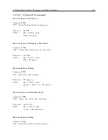
Set Voltage Amplitude Correction
Command:
v:kRV
“v:kRV” sets the system voltage amplitude correction.
Response:
C
Where:
v = Voltage correction per unit with 1.000000 equal to no correction.
k = Security Key (e.g. 1088)
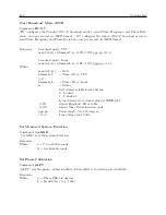
Return Time, Frequency, Phase Deviation with UTC Time
Command:
nPD
“nPD” returns the System Time, Frequency and Phase Deviation with a UTC time reference, at
each issuance of the command.
Response:
(when n = 0) mm/dd/yyyy hh:mm:ssU ss +f.fff +t.tttt ppp.pp vvv.vv
C
(when n = 1) mm/dd/yyyy hh:mm:ssL ss +f.fff +t.tttt ppp.pp vvv.vv
C
Where:
mm/dd/yyyy
= Date
hh:mm:ssU
= Time of Day, UTC
(or)
hh:mm:ssL
= Time of Day, Local
ss
= Status (0 = Locked, 1 = Unlocked)
(first character is Reference Status:)
(second character is clock status per IEEE 1344)
+f.fff
signed Frequency Error in Hz.
+t.tttt
signed Time Deviation in seconds.
ppp.pp
Phase Angle, 0 to 360 degrees.
vvv.vv
Line voltage, rms Volts.
Содержание 1088A
Страница 4: ...iv ...
Страница 6: ...vi ...
Страница 18: ...xviii LIST OF FIGURES ...
Страница 23: ...1 4 Attaching Rack Mount Ears to 1088A B Series Clocks 3 Figure 1 2 Attaching Rack Mount Ears ...
Страница 24: ...4 Unpacking the Clock ...
Страница 32: ...12 Front and Rear Panels ...
Страница 38: ...18 Connecting Inlet Power Input and Output Signals ...
Страница 41: ...4 1 GPS Antenna Installation 21 Figure 4 2 Antenna Mounting Bracket Figure 4 3 Antenna Mounting with AS0044600 ...
Страница 46: ...26 GPS Antenna and Cable Information ...
Страница 48: ...28 Setting Internal Jumpers Figure 5 1 Model 1088B Main Board ...
Страница 76: ...56 The Setup Menus ...
Страница 112: ...92 Serial Communication and Command Set ...
Страница 127: ...B 4 Physical Dimensions 107 Figure B 1 Suggested Mounting of the AS0094500 Surge Arrester ...
Страница 128: ...108 Using Surge Arresters ...
Страница 137: ...C 5 Option 04 Parallel BCD Output 117 C 5 2 Option 04 Firmware Setup Figure C 2 Option 04 Firmware Setup ...
Страница 145: ...C 5 Option 04 Parallel BCD Output 125 Figure C 4 Option 04 Output Jumper Settings ...
Страница 146: ...126 Options List Figure C 5 Option 04 Board Layout and Jumper Locations ...
Страница 165: ...C 12 Option 17 Parallel BCD Output and Second RS 232 Port 145 Figure C 11 Option 17 Output Jumper Settings ...
Страница 166: ...146 Options List Figure C 12 Option 17 Board Layout and Jumper Locations ...
Страница 176: ...156 Options List C 14 5 Typical Network Configuration Figure C 15 Option 18 Network Configuration ...
Страница 187: ...C 16 Option 20A Four Fiber Optic Outputs 167 Figure C 22 Option 20A Jumper Locations ...
Страница 194: ...174 Options List Figure C 24 Option 23 Internal Jumper Setup ...
Страница 196: ...176 Options List Figure C 25 Option 27 Jumper Locations ...
Страница 214: ...194 Options List Figure C 28 Option 29 Connector Signal Locations ...
Страница 270: ...250 Options List ...


