7.4 Connecting Outputs
63
with no loads) is approximately 10 Vpp, so any connected loads will cause the available voltage to
drop. It is a simple task to compute the available output voltage (Vpp) with a known current.
(7.2)
V pp
= 10
V pp
−
I
×
557
Ohms
Therefore, if you had 10 mA of load current (I load) the available voltage (Vpp) would be 4.43
Vpp. If the load current equals 15 mA, then the available voltage would be 1.64 Vpp. So, you can
see how the increasing load current (i.e number of loads) affects the available drive voltage at the
clock output. See also Table 7.1.
7.4.6
Wire Losses
Another factor affecting the available voltage is the resistive losses through the cabling. Wire has a
certain resistivity associated with it that is determined by its metallic composition, and resistance
determined by the diameter and length. For example, single-strand, 22 AWG (bare, enamel-coated)
copper wire has a resistance of approximately 19.6 ohms per 1000 feet. To compute the loss we
must include both wires in the connection, signal and return. For coaxial cabling, the resistance of
the center conductor is rated differently than the shield. For a twisted pair, both of them should
essentially have the same resistance per cut length. If we use a twisted pair of 22 AWG (copper as
above), then the available voltage (at 10 mA of current) for 500 feet of wire including the source
resistor would be:
(7.3)
V pp available
= 10
−
I
×
557
source
−
I
×
19
.
6
wire
= 1
.
35
V pp
So, you can see that most of the drive voltage is lost with 15 mA of current and 500 feet of 22 AWG
twisted pair transmission line; this includes the voltage losses at the source resistor. 1.35 Vpp may
very likely not be detected by the decoder in some IED’s. Remember to make your cable runs as
short as possible, to use a larger diameter cable, and to carefully distribute the loads.
7.4.7
Voltage Matching for Modulated IRIG-B
With modulated IRIG-B, it was mentioned that certain decoders are very intolerant of drive voltage
variation. If the IED specification says that the acceptable voltage range is 3.3 Vpp
±
0.5 volt, and
the available voltage is high, then you must reduce the voltage using a dropping resistor (
R
drop
).
The value of the dropping resistor is determined by dividing the difference voltage (
V
dif f
) by the
device current (
I
dev
). For example, suppose that the available voltage is 4.43 Vpp, the (nominal)
acceptable voltage is 3.3 Vpp, and the device current is 10 mA. Determine the dropping resistor
value.
(7.4)
R
drop
=
V
dif f
÷
I
dev
= (4
.
43
−
3
.
3)
÷
0
.
01 = 113
Ohms
The Power dissipation (P) is:
(7.5)
P
=
I
2
R
= 0
.
01
2
×
113 = 0
.
011
W atts
In this example, an eighth-watt resistor should work fine.
For a voltage that is too low, the modulated IRIG-B signal level must be increased by some other
means, such as (1) distributing the load differently to reduce the current (raising the available
voltage), (2) by reducing the cable loss by increasing the wire size, or (3) by using an amplifier.
Содержание 1088A
Страница 4: ...iv ...
Страница 6: ...vi ...
Страница 18: ...xviii LIST OF FIGURES ...
Страница 23: ...1 4 Attaching Rack Mount Ears to 1088A B Series Clocks 3 Figure 1 2 Attaching Rack Mount Ears ...
Страница 24: ...4 Unpacking the Clock ...
Страница 32: ...12 Front and Rear Panels ...
Страница 38: ...18 Connecting Inlet Power Input and Output Signals ...
Страница 41: ...4 1 GPS Antenna Installation 21 Figure 4 2 Antenna Mounting Bracket Figure 4 3 Antenna Mounting with AS0044600 ...
Страница 46: ...26 GPS Antenna and Cable Information ...
Страница 48: ...28 Setting Internal Jumpers Figure 5 1 Model 1088B Main Board ...
Страница 76: ...56 The Setup Menus ...
Страница 112: ...92 Serial Communication and Command Set ...
Страница 127: ...B 4 Physical Dimensions 107 Figure B 1 Suggested Mounting of the AS0094500 Surge Arrester ...
Страница 128: ...108 Using Surge Arresters ...
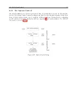
Страница 137: ...C 5 Option 04 Parallel BCD Output 117 C 5 2 Option 04 Firmware Setup Figure C 2 Option 04 Firmware Setup ...
Страница 145: ...C 5 Option 04 Parallel BCD Output 125 Figure C 4 Option 04 Output Jumper Settings ...
Страница 146: ...126 Options List Figure C 5 Option 04 Board Layout and Jumper Locations ...
Страница 165: ...C 12 Option 17 Parallel BCD Output and Second RS 232 Port 145 Figure C 11 Option 17 Output Jumper Settings ...
Страница 166: ...146 Options List Figure C 12 Option 17 Board Layout and Jumper Locations ...
Страница 176: ...156 Options List C 14 5 Typical Network Configuration Figure C 15 Option 18 Network Configuration ...
Страница 187: ...C 16 Option 20A Four Fiber Optic Outputs 167 Figure C 22 Option 20A Jumper Locations ...
Страница 194: ...174 Options List Figure C 24 Option 23 Internal Jumper Setup ...
Страница 196: ...176 Options List Figure C 25 Option 27 Jumper Locations ...
Страница 214: ...194 Options List Figure C 28 Option 29 Connector Signal Locations ...
Страница 270: ...250 Options List ...


