Diagnostic & Troubleshooting 6 - 5
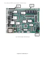
The overall layout of PCB A2 is shown in Figure 6.1 for further reference.
Fig 6.1 Electronic Bypass Control Board Layout
Customer
Connection
Terminals
Connector
For cable to
Keypad
Customer
120V
Circuit Fuse
Customer
Configuration
Switches
Connector
For cable to
Drive
CPLD
Logic
Processor
Option Port
Connector
Option Port
Connector
Connectors
to Panel
Wiring
Harnesses
Main
Control
Fuse
Power
Supply
Circuits
Mounting
Holes
5 Places
Summary of Contents for E7LBA002
Page 1: ...E7L Drive Bypass Technical Manual Model E7L Document Number TM E7L 01 ...
Page 8: ...Introduction vi Notes ...
Page 12: ...Table of Contents x Notes ...
Page 54: ...Electrical Installation 2 22 Wiring Diagram ...
Page 55: ...Electrical Installation 2 23 ...
Page 87: ...Start Up and Operation 4 9 Notes ...
Page 202: ...Diagnostic Troubleshooting 6 30 Notes ...
Page 248: ...Capacity Related Parameters B 6 Notes ...
Page 279: ...Communications D 27 Note ...
Page 280: ...Communications D 28 ...
Page 292: ...Spare Parts F 6 ...
Page 304: ...Index 12 ...
Page 305: ......

