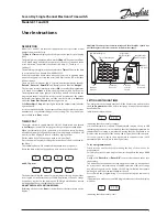
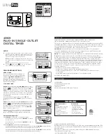
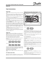
H3BA
H3BA
290
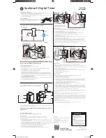
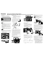
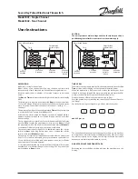
Connection
Contact Signal Inputs
Connect the start input contact between terminals
B
and
F
, the reset
input contact between terminals
B
and
G
, the gate input contact be-
tween terminals
B
and
E
, respectively. For each signal input con-
tact, use a gold-plated contact of high contact reliability. Be sure that
these input signals satisfy the following requirements:
1. A resistance of 1 k
$
(max.) when the contact makes.
2. A residual voltage of 1 V (max.) when the contact makes.
Solid-state Signal Inputs
Connect the start input transistor between terminals
B
and
F
, the re-
set input transistor between terminals
B
and
G
, the gate input tran-
sistor between terminals
B
and
E
, respectively.
For signal input, use an open collector transistor with characteris-
tics: V
CEO
= 20 V min., V
CE(S)
= 1 V max., I
C
= 50 mA min. and I
CBO
=
0.5
&
A max. In addition, be sure that the input signals satisfy the fol-
lowing requirements:
1. A resistance of 1 k
$
(max.) when the resister is ON.
2. A residual voltage of 1 V (max.) when the transistor is ON
3. A resistance of 200 k
$
(min.) when the transistor is OFF
From a solid-state circuit (proximity sensor, photoelectric sensor, or
the like) with rated power supply voltage ranging from 6 to 30 VDC,
input signals can also be applied by other than an open collector
type transistor as shown in the following diagram.
Solid-state circuit (proximity sensor,
photoelectric sensor, etc.)
Note:
Except for the wiring for the power supply circuitry, avoid
the laying of input signal wires in parallel or in the same con-
duit with high-tension or power lines. It is recommended to
use shielded wires or wiring with independent metal con-
duits for the shortest possible distance.