Rev. 3.0, 04/02, page 510 of 1064
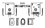
Bus cycle
(When Bcyc : Pcyc = 1 : 1)
CKIO
Source address
Read
Read
Read
D[31:0]
Write
Write
Write
Source address
Source address
A[25:0]
Destination address
Destination address
Destination address
CPU
DMAC
CPU
DMAC
CPU
DMAC
T1
T2
T1
T2
T1
T2
On-chip
peripheral
address bus
On-chip
peripheral
data bus
Figure 14.17 Dual Address Mode/Cycle Steal Mode
External Bus
On-Chip SCI (Level Detection)
Summary of Contents for SH7751
Page 39: ...Rev 3 0 04 02 page xxxviii of xxxviii ...
Page 89: ...Rev 3 0 04 02 page 50 of 1064 ...
Page 157: ...Rev 3 0 04 02 page 118 of 1064 ...
Page 193: ...Rev 3 0 04 02 page 154 of 1064 ...
Page 225: ...Rev 3 0 04 02 page 186 of 1064 ...
Page 253: ...Rev 3 0 04 02 page 214 of 1064 ...
Page 301: ...Rev 3 0 04 02 page 262 of 1064 ...
Page 343: ...Rev 3 0 04 02 page 304 of 1064 ...
Page 607: ...Rev 3 0 04 02 page 568 of 1064 ...
Page 671: ...Rev 3 0 04 02 page 632 of 1064 ...
Page 745: ...Rev 3 0 04 02 page 706 of 1064 ...
Page 767: ...Rev 3 0 04 02 page 728 of 1064 ...
Page 1061: ...Rev 3 0 04 02 page 1022 of 1064 NMI tNMIL tNMIH Figure 23 69 NMI Input Timing ...
Page 1069: ...Rev 3 0 04 02 page 1030 of 1064 ...
Page 1103: ...Rev 3 0 04 02 page 1064 of 1064 ...