SMARC T335x Carrier Board Hardware Design Guide, Document Revision 1.2
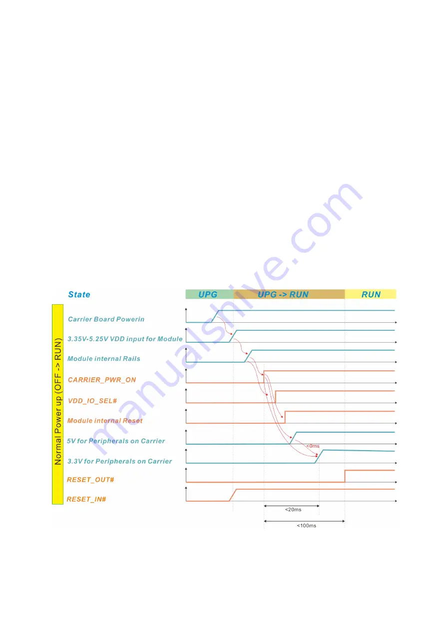
VDD_IO_SEL#
as soon as the main voltage supply is applied to the module
and all module supplies necessary for module booting are up. This is to ensure
that the module is powered before the main body of carrier circuits (those
outside the power and power control path on the carrier) and the
VDD_IO
of
module and carrier is matching. The module will continue to assert signal
RESET_OUT#
after the release of
CARRIER_PWR_ON
and
VDD_IO_SEL#
,
for a period sufficient time (at least 10ms) to allow carrier power circuits that
the peripheral supplies need to ramp up.
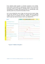
The peripheral power rails on the carrier board need to ramp up in a correct
sequence. The sequence starts normally with the highest voltage (e.g. 5V)
followed by the lower voltages (e.g. 3.3V then 1.5V and so on). Peripherals
normally require that a lower voltage rails is never present if a higher rail is
missing. Check the datasheet of all peripheral components on the carrier
board for a proper sequencing. The
T335X
modules guarantees to apply the
reset output
RESET_OUT#
not earlier than 100ms after the
CARRIER_PWR_ON
goes high. This gives the carrier board a sufficient time
for ramping up all power rails.
SDIO_PWR_EN
signal have to be pull up to
3.3V on carrier if users would like to have SD boot up functionality.
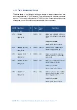
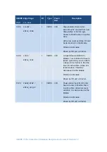
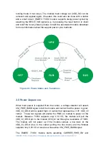
Figure 40: Power-Up Sequence

