SMARC T335x Carrier Board Hardware Design Guide, Document Revision 1.2
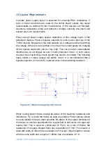
Copper foils on the outer layers of a PCB (top and bottom layer) often are
thicker due to the via plating process. A common value is one ounce of copper
per square foot. This equals to a thickness of 35
μ
m. The traces of on such
layers have half the electrical resistance, which is 0.5m
for a square shaped
trace. Also consider the electrical resistance of vias. For every ampere of
current, place at least one via.
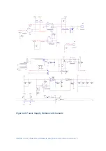
3.7 Reference Schematics
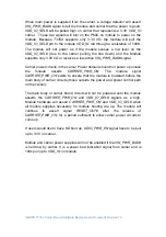
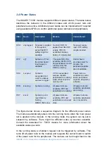
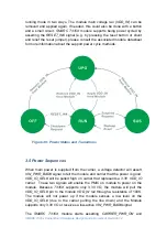
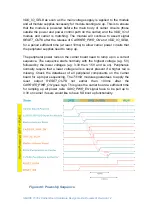
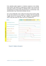
It is possible to reach a suitable power up sequence by cascading the power
good (e.g.
VIN_PWR_BAD#
) output signals of the buck regulators with enable
signal of the next regulator. The
CARRIER_PWR_ON
output features a pull up
resistor on the
T335X
module. An additional pull up resistor can be optionally
placed on the carrier board. This pull up resistor is only needed to prevent
unwanted enabling of the peripheral voltages if the module is not inserted. For
designs in which the module is never removed, this pull up is not required.
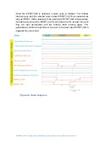
The
RESET_IN#
and
RESET_OUT#
can also have additional pull up resistors
on the carrier board for the same reasons.

