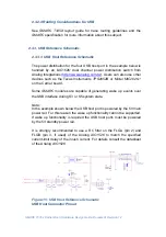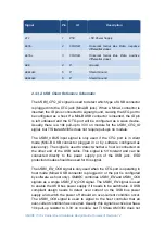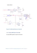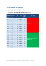
SMARC T335x Carrier Board Hardware Design Guide, Document Revision 1.2
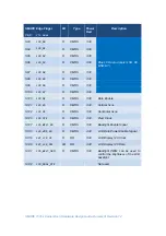
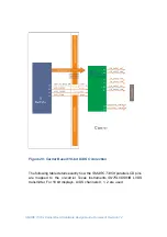
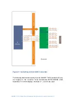
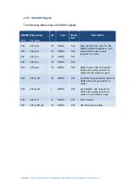
SMARC Module
Edge Golden Finger
LVDS Transmitter (TI
SN75LVDS83B)
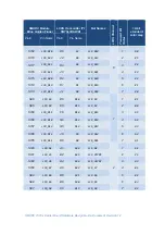
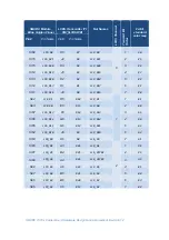
Net Names
L
V
DS Ch
ann
e
l
Tr
a
n
s
m
it
B
it
Order
18-bit
standard
color map
Pin#
Pin Name
Pin#
Pin Name
Not Used
Not
Used
A5
D23
Not
Used
3
1
Not
Used
S94
LCD_D1
D6
D17
LCD_D1
2
Not
Used
S93
LCD_D0
E6
D16
LCD_D0
3
Not
Used
S103
LCD_D9
H6
D11
LCD_D9
4
Not
Used
S102
LCD_D8
H4
D10
LCD_D8
5
Not
Used
S112
LCD_D17
K4
D5
LCD_D17
6
Not
Used
S111
LCD_D16
J1
D27
LCD_D16
7
Not
Used
S123
LCD_PCK
A2
CLKIN
LCD_PCLK
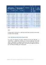
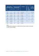
Note:
If unused pin is not driven to a valid logic level, then an external connection
to GND is recommended.
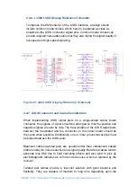
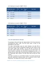
2.4.6. Carrier Based 24 bit Color Depth LVDS
For 24 bit color depths, four LVDS channels are used (24 data bits + 3
control bits + 1 unused bit = 28 bits, or 4 x 7) plus a clock pair. The LVDS
clock is transmitted on a separate LVDS pair. The LVDS clock period is 7
times longer than the pixel clock period. The LVDS clock edges are off from
the 7 bit frame boundaries by 2 pixel periods.

