SMARC T335x Carrier Board Hardware Design Guide, Document Revision 1.2
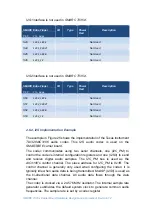
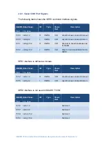
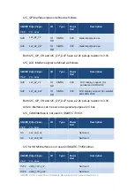
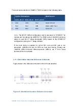
SPI1
interface signal is defined as follows.
SMARC Edge Finger
I/O
Type
Power
Rail
Description
Pin#
Pin
Name
P54
SPI1_CS0#
IO
CMOS
3.3V
SPI1 Master Chip Select 0 output
P55
SPI1_CS1#
IO
CMOS
3.3V
SPI1 Master Chip Select 1 output
P56
SPI1_CK
IO
CMOS
3.3V
SPI1 Master Clock output
P57
SPI1_DIN
I
CMOS
3.3V
SPI1 Master Data input (input to
CPU, output from SPI device)
P58
SPI1_DO
IO
CMOS
3.3V
SPI1 Master Data output (output
from CPU, input to SPI device)
2.9.2. SPI Interface Implementation Guidelines
SPI Devices communicate using a master/slave relationship, in which the
master initiates the data frame. When the master generates a clock and
selects a slave device, data may be transferred in either or both directions
simultaneously. In fact, as far as SPI is concerned, data are always
transferred in both directions.
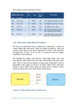
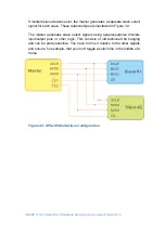
SPI specifies four signals: clock (SCLK); master data output, slave data
input (MOSI); master data input, slave data output (MISO); and slave select
(ÇS). Figure 31 shows these signals in a single-slave configuration. SCLK is
generated by the master and input to all slaves. MOSI carries data from
master to slave. MISO carries data from slave back to master. A slave
device is selected when the master asserts its ÇS signal.
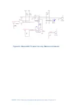
Figure 31: SPI with Single-Slave Configuration

