SMARC T335x Carrier Board Hardware Design Guide, Document Revision 1.2
3.6 Layout Requirements
A proper power supply layout is essential for ensuring EMC compliance. If
buck or boost converters are used on the carrier board, ensure any layout
requirements as defined by the manufacturer of the devices are followed.
Generally, application notes and reference designs carefully document and
explain any such requirements.
Place enough power supply bypass capacitors on the voltage inputs of the
peripheral devices. Place a bypass capacitor to each power input pin of the
T335X
module. Be aware of the total capacity on a voltage rail when switching
the voltage. If the rails are switched on too fast, the current peaks for charging
all the bypass capacitors can be very high. This can produce unacceptable
disturbances or can trigger an over current protection circuit. In such cases,
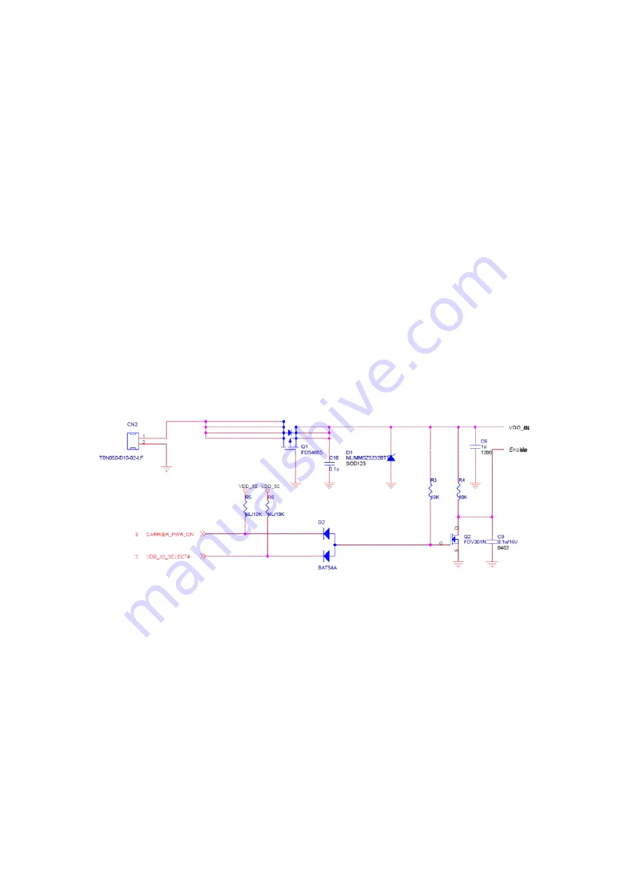
the slew rate of switching circuits speed may need to be limited. The following
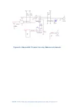
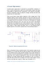
figure shows a simple voltage rail switch circuit. It is recommended that a
bypass capacitor (C10 and C6) is placed close to the switching transistor.
Figure 43: Simple Voltage Switch Circuit
When routing power traces, always be aware of the electrical resistance and
inductance. Try to make the traces as wide as possible. Power planes should
be used instead of traces when possible. Be aware of the copper thickness of
the traces. A common specification for copper foils is half ounce of copper per
square foot. This is equal to a thickness of 17
μ
m. As a rule of thumb, the
resistance of a square shaped trace has a resistance of 1m
. This means, a
trace with width of 100
μ
m has a resistance of 1m
per 100
μ
m length or a trace
with the same width and a length of 100mm has a resistance of 1
.

