Semiconductor Group
6-14
1999-04-01
On-Chip Peripheral Components
C541U
6.1.3.3
Read-Modify-Write Feature of Ports 1,2 and 3
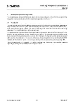
Some port-reading instructions read the latch and others read the pin. The instructions reading the
latch rather than the pin read a value, possibly change it, and then rewrite it to the latch. These are
called "read-modify-write"- instructions, which are listed in table 6-2. If the destination is a port or a
port pin, these instructions read the latch rather than the pin. Note that all other instructions which
can be used to read a port, exclusively read the port pin. In any case, reading from latch or pin,
respectively, is performed by reading the SFR P0, P1, P2 and P3; for example, "MOV A, P3" reads
the value from port 3 pins, while "ANL P3, #0AAH" reads from the latch, modifies the value and
writes it back to the latch.
It is not obvious that the last three instructions in table 6-2 are read-modify-write instructions, but
they are. The reason is that they read the port byte, all 8 bits, modify the addressed bit, then write
the complete byte back to the latch.
The reason why read-modify-write instructions are directed to the latch rather than the pin is to avoid
a possible misinterpretation of the voltage level at the pin. For example, a port bit might be used to
drive the base of a transistor. When a "1" is written to the bit, the transistor is turned on. If the CPU
then reads the same port bit at the pin rather than the latch, it will read the base voltage of the
transistor (approx. 0.7 V, i.e. a logic low level!) and interpret it as "0". For example, when modifying
a port bit by a SETB or CLR instruction, another bit in this port with the above mentioned
configuration might be changed if the value read from the pin were written back to the latch.
However, reading the latch rater than the pin will return the correct value of "1".
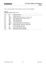
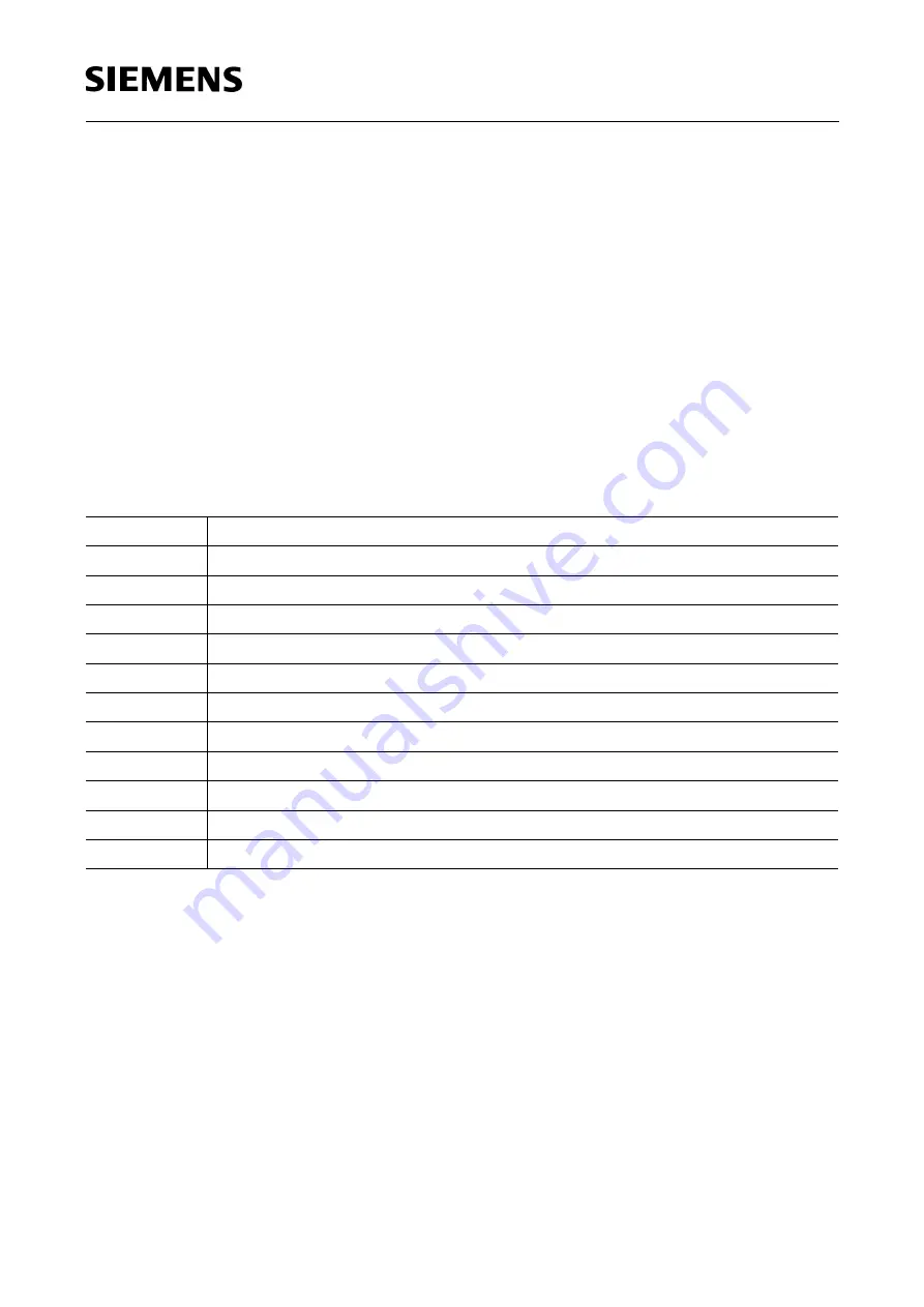
Table 6-2
Read-Modify-Write"- Instructions
Instruction
Function
ANL
Logic AND; e.g. ANL P1, A
ORL
Logic OR; e.g. ORL P2, A
XRL
Logic exclusive OR; e.g. XRL P3, A
JBC
Jump if bit is set and clear bit; e.g. JBC P1.1, LABEL
CPL
Complement bit; e.g. CPL P3.0
INC
Increment byte; e.g. INC P1
DEC
Decrement byte; e.g. DEC P1
DJNZ
Decrement and jump if not zero; e.g. DJNZ P3, LABEL
MOV Px.y,C
Move carry bit to bit y of port x
CLR Px.y
Clear bit y of port x
SETB Px.y
Set bit y of port x
Содержание C541U
Страница 1: ... 8 LW 026 0LFURFRQWUROOHU 8VHU V 0DQXDO http www siem ens d Sem iconductor ...
Страница 7: ......
Страница 21: ...Semiconductor Group 2 6 1997 10 01 Fundamental Structure C541U ...
Страница 37: ...Semiconductor Group 4 6 1997 10 01 External Bus Interface C541U ...
Страница 133: ...Semiconductor Group 6 88 1999 04 01 On Chip Peripheral Components C541U ...
Страница 163: ...Semiconductor Group 8 8 1997 10 01 Fail Safe Mechanisms C541U ...
Страница 185: ...Semiconductor Group 10 14 1997 10 01 OTP Memory Operation C541U ...
Страница 192: ...Semiconductor Group 12 7 Index C541U ...

