Semiconductor Group
6-12
1999-04-01
On-Chip Peripheral Components
C541U
6.1.3 Port Handling
6.1.3.1
Port Timing
When executing an instruction that changes the value of a port latch, the new value arrives at the
latch during S6P2 of the final cycle of the instruction. However, port latches are only sampled by
their output buffers during phase 1 of any clock period (during phase 2 the output buffer holds the
value it noticed during the previous phase 1). Consequently, the new value in the port latch will not
appear at the output pin until the next phase 1, which will be at S1P1 of the next machine cycle.
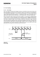
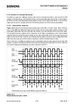
When an instruction reads a value from a port pin (e.g. MOV A, P1) the port pin is actually sampled
in state 5 phase 1 or phase 2 depending on port and alternate functions. Figure 6-9 illustrates this
port timing. lt must be noted that this mechanism of sampling once per machine cycle is also used
if a port pin is to detect an "edge", e.g. when used as counter input. In this case an "edge" is detected
when the sampled value differs from the value that was sampled the cycle before. Therefore, there
must be met certain requirements on the pulse length of signals in order to avoid signal "edges" not
being detected. The minimum time period of high and low level is one machine cycle, which
guarantees that this logic level is noticed by the port at least once.
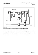
Figure 6-9
Port Timing
S4
P1
P2
P1
P2
S5
P1
P2
S6
P1
P2
S1
P1
P2
S2
XTAL2
S3
P1
P2
Port
Input sampled:
e.g.: MOV A, P1
or
Old Data
New Data
P1 Active
(driver Transistor)
MCT03397
Содержание C541U
Страница 1: ... 8 LW 026 0LFURFRQWUROOHU 8VHU V 0DQXDO http www siem ens d Sem iconductor ...
Страница 7: ......
Страница 21: ...Semiconductor Group 2 6 1997 10 01 Fundamental Structure C541U ...
Страница 37: ...Semiconductor Group 4 6 1997 10 01 External Bus Interface C541U ...
Страница 133: ...Semiconductor Group 6 88 1999 04 01 On Chip Peripheral Components C541U ...
Страница 163: ...Semiconductor Group 8 8 1997 10 01 Fail Safe Mechanisms C541U ...
Страница 185: ...Semiconductor Group 10 14 1997 10 01 OTP Memory Operation C541U ...
Страница 192: ...Semiconductor Group 12 7 Index C541U ...

