Semiconductor Group
6-15
1999-04-01
On-Chip Peripheral Components
C541U
6.2
Timers/Counters
The C541U contains two 16-bit timers/counters, timer 0 and 1, which are useful in many
applications for timing and counting.
In "timer" function, the timer register is incremented every machine cycle. Thus one can think of it
as counting machine cycles. Since a machine cycle consists of 6 oscillator periods, the counter rate
is 1/6 of the oscillator frequency.
In "counter" function, the timer register is incremented in response to a 1-to-0 transition (falling
edge) at its corresponding external input pin, T0 or T1 (alternate functions of P3.4 and P3.5). In this
function the external input is sampled during S5P2 of every machine cycle. When the samples show
a high in one cycle and a low in the next cycle, the count is incremented. The new count value
appears in the register during S3P1 of the cycle following the one in which the transition was
detected. Since it takes two machine cycles (12 oscillator periods) to recognize a 1-to-0 transition,
the maximum count rate is 1/12 of the oscillator frequency. There are no restrictions on the duty
cycle of the external input signal, but to ensure that a given level is sampled at least once before it
changes, it must be held for at least one full machine cycle.
6.2.1
Timer/Counter 0 and 1
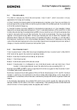
Timer / counter 0 and 1 of the C541U are fully compatible with timer / counter 0 and 1 of the 80C51/
C501 and can be used in the same four operating modes:
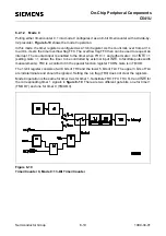
Mode 0: 8-bit timer/counter with a divide-by-32 prescaler
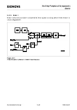
Mode 1: 16-bit timer/counter
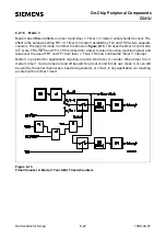
Mode 2: 8-bit timer/counter with 8-bit auto-reload
Mode 3: Timer/counter 0 is configured as one 8-bit timer/counter and one 8-bit timer; Timer/
counter 1 in this mode holds its count. The effect is the same as setting TR1 = 0.
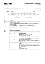
External inputs INT0 and INT1 can be programmed to function as a gate for timer/counters 0 and 1
to facilitate pulse width measurements.
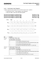
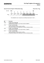
Each timer consists of two 8-bit registers (TH0 and TL0 for timer/counter 0, TH1 and TL1 for timer/
counter 1) which may be combined to one timer configuration depending on the mode that is
established. The functions of the timers are controlled by two special function registers TCON and
TMOD.
In the following descriptions the symbols TH0 and TL0 are used to specify the high-byte and the
low-byte of timer 0 (TH1 and TL1 for timer 1, respectively). The operating modes are described and
shown for timer 0. If not explicity noted, this applies also to timer 1.
Содержание C541U
Страница 1: ... 8 LW 026 0LFURFRQWUROOHU 8VHU V 0DQXDO http www siem ens d Sem iconductor ...
Страница 7: ......
Страница 21: ...Semiconductor Group 2 6 1997 10 01 Fundamental Structure C541U ...
Страница 37: ...Semiconductor Group 4 6 1997 10 01 External Bus Interface C541U ...
Страница 133: ...Semiconductor Group 6 88 1999 04 01 On Chip Peripheral Components C541U ...
Страница 163: ...Semiconductor Group 8 8 1997 10 01 Fail Safe Mechanisms C541U ...
Страница 185: ...Semiconductor Group 10 14 1997 10 01 OTP Memory Operation C541U ...
Страница 192: ...Semiconductor Group 12 7 Index C541U ...

