Semiconductor Group
6-9
1999-04-01
On-Chip Peripheral Components
C541U
6.1.1.4
Port 0 and Port 2 used as Address/Data Bus
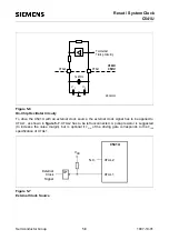
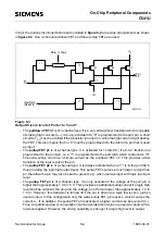
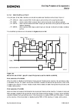
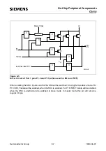
As shown in figure 6-6 and below in figure 6-7, the output drivers of ports 0 and 2 can be switched
to an internal address or address/data bus for use in external memory accesses. In this application
they cannot be used as general purpose I/O, even if not all address lines are used externally. The
switching is done by an internal control signal dependent on the input level at the EA pin and/or the
contents of the program counter. If the ports are configured as an address/data bus, the port latches
are disconnected from the driver circuit. During this time, the P2 SFR remains unchanged while the
P0 SFR has 1’s written to it. Being an address/data bus, port 0 uses a pullup FET as shown in
figure 6-6. When a 16-bit address is used, port 2 uses the additional strong pullups p1 to emit 1’s
for the entire external memory cycle instead of the weak ones (p2 and p3) used during normal port
activity.
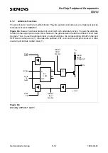
Figure 6-7
Port 2 Circuitry
MCS02123
D
CLK
Bit
Latch
Q
Q
Control
Addr.
MUX
Internal
Pull Up
Arrangement
V
CC
Port
Pin
Int. Bus
Write to
Pin
Read
Latch
Latch
Read
=1
Содержание C541U
Страница 1: ... 8 LW 026 0LFURFRQWUROOHU 8VHU V 0DQXDO http www siem ens d Sem iconductor ...
Страница 7: ......
Страница 21: ...Semiconductor Group 2 6 1997 10 01 Fundamental Structure C541U ...
Страница 37: ...Semiconductor Group 4 6 1997 10 01 External Bus Interface C541U ...
Страница 133: ...Semiconductor Group 6 88 1999 04 01 On Chip Peripheral Components C541U ...
Страница 163: ...Semiconductor Group 8 8 1997 10 01 Fail Safe Mechanisms C541U ...
Страница 185: ...Semiconductor Group 10 14 1997 10 01 OTP Memory Operation C541U ...
Страница 192: ...Semiconductor Group 12 7 Index C541U ...


