Semiconductor Group
10-7
1997-10-01
OTP Memory Operation
C541U
10.5
Program / Read OTP Memory Bytes
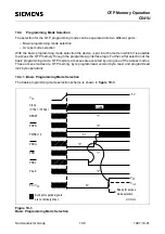
The program/read OTP memory byte access mode is defined by PMSEL1,0 = 1,1. It is initiated
when the PMSEL1,0 = 1,1 is valid at the rising edge of PALE. With the falling edge of PALE the
upper addresses A8-A12 of the 13-bit OTP memory address are latched. After A8-A12 has been
latched, A0-A7 is put on the address bus (port 2). A0-A7 must be stable when PROG is low or PRD
is low. If subsequent OTP address locations are accessed with constant address information at the
high address lines A8-12, A8-A12 must only be latched once (page address mechanism).
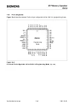
Figure 10-4 shows a typical OTP memory programming cycle with a following OTP memory read
operation. In this example A0-A12 of the read operation are identical to A8-A12 of the preceeding
programming operation.
Figure 10-4
C541U Programming / VerifyOTP Memory Access Waveform
If the address lines A8-A12 must be updated, PALE must be activated for the latching of the new A8-
A12 value. Control, address, and data information must only be switched when the PROG and PRD
signals are at high level. The PALE high pulse must always be executed if a different access mode
has been used prior to the actual access mode.
D0 - D7
min. 100 s
µ
D0 - D7
A8-A12
A0-A7
1,1
PMSEL1,0
Port 2
PALE
Port 0
PROG
PRD
MCT03419
min.
100 ns
Содержание C541U
Страница 1: ... 8 LW 026 0LFURFRQWUROOHU 8VHU V 0DQXDO http www siem ens d Sem iconductor ...
Страница 7: ......
Страница 21: ...Semiconductor Group 2 6 1997 10 01 Fundamental Structure C541U ...
Страница 37: ...Semiconductor Group 4 6 1997 10 01 External Bus Interface C541U ...
Страница 133: ...Semiconductor Group 6 88 1999 04 01 On Chip Peripheral Components C541U ...
Страница 163: ...Semiconductor Group 8 8 1997 10 01 Fail Safe Mechanisms C541U ...
Страница 185: ...Semiconductor Group 10 14 1997 10 01 OTP Memory Operation C541U ...
Страница 192: ...Semiconductor Group 12 7 Index C541U ...

