Semiconductor Group
5-5
1997-10-01
Reset / System Clock
C541U
5.3
Hardware Reset Timing
This section describes the timing of the hardware RESET signal.
The input pin RESET is sampled once during each machine cycle. This happens in state 5 phase 2.
Thus, the external reset signal is synchronized to the internal CPU timing. When RESET is found
active (high level) the internal reset procedure is started. It needs two complete machine cycles to
put the complete device to its correct reset state, i.e. all special function registers contain their
default values, the port latches contain 1’s etc. Note that this reset procedure is also performed if
there is no clock available at the device. (This is done by the oscillator watchdog, which provides an
auxiliary clock for performing a perfect reset without clock at the XTAL1 and XTAL2 pins). The
RESET signal must be active for at least two machine cycles; after this time the C541U remains in
its reset state as long as the signal is active. When the signal goes inactive this transition is
recognized in the following state 5 phase 2 of the machine cycle. Then the processor starts its
address output (when configured for external program memory) in the following state 5 phase 1.
One phase later (state 5 phase 2) the first falling edge at pin ALE occurs.
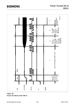
Figure 5-3 shows this timing for a configuration with EA = 0 (external program memory). Thus,
between the release of the RESET signal and the first falling edge at ALE there is a time period of
at least one machine cycle but less than two machine cycles.
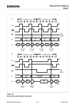
Figure 5-3
CPU Timing after Reset
MCT02092
S4
S5
S6
S1
S2
S3
S4
S5
S6
S1
S2
S3
S4
S5
S6
S1
S2
P1 P2
PCL
OUT
PCH
OUT
PCH
OUT
One Machine Cycle
RESET
P0
P2
ALE
Inst.
in
OUT
PCL
Содержание C541U
Страница 1: ... 8 LW 026 0LFURFRQWUROOHU 8VHU V 0DQXDO http www siem ens d Sem iconductor ...
Страница 7: ......
Страница 21: ...Semiconductor Group 2 6 1997 10 01 Fundamental Structure C541U ...
Страница 37: ...Semiconductor Group 4 6 1997 10 01 External Bus Interface C541U ...
Страница 133: ...Semiconductor Group 6 88 1999 04 01 On Chip Peripheral Components C541U ...
Страница 163: ...Semiconductor Group 8 8 1997 10 01 Fail Safe Mechanisms C541U ...
Страница 185: ...Semiconductor Group 10 14 1997 10 01 OTP Memory Operation C541U ...
Страница 192: ...Semiconductor Group 12 7 Index C541U ...

