Semiconductor Group
10-4
1997-10-01
OTP Memory Operation
C541U
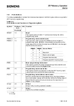
A0/A8 -
A7
24 - 31
I
Address lines
P2.0-7 are used as multiplexed address input lines A0-A7 and A8-
A12. A8-A12 must be latched with PALE.
PSEN
32
I
Program store enable
This input must be at static “0“ level during the whole programming
mode.
PROG
33
I
Programming mode write strobe
This input is used in programming mode as a write strobe for OTP
memory program and lock bit write operations During basic
programming mode selection a low level must be applied to PROG.
EA/V
PP
35
I
External Access / Programming voltage
This pin must be at 11.5 V (V
PP
) voltage level during programming
of an OTP memory byte or lock bit. During an OTP memory read
operation this pin must be at high level (V
IH
). This pin is also used
for basic programming mode selection. At basic programming
mode selection a low level must be applied to EA/V
PP
.
D0 - 7
43 - 36
I/O
Data lines 0-7
During programming mode, data bytes are read or written from or
to the C541U via the bidirectional D0-7 lines which are located at
port 0.
V
SS
9, 22
–
Circuit ground potential
must be applied to these pins in programming mode.
V
DD
8, 23
–
Power supply terminal
must be applied to these pins in programming mode.
N.C.
1 - 7, 12,,
34, 44
–
Not Connected
These pins should not be connected in programming mode.
GND
17 - 19
I
Ground pins
In programming mode these pins must be connected to
V
IL
level.
*) I = Input
O = Output
Table 10-1
Pin Definitions and Functions in Programming Mode (cont’d)
Symbol
Pin Num-
bers
I/O*) Function
P-LCC-44
Содержание C541U
Страница 1: ... 8 LW 026 0LFURFRQWUROOHU 8VHU V 0DQXDO http www siem ens d Sem iconductor ...
Страница 7: ......
Страница 21: ...Semiconductor Group 2 6 1997 10 01 Fundamental Structure C541U ...
Страница 37: ...Semiconductor Group 4 6 1997 10 01 External Bus Interface C541U ...
Страница 133: ...Semiconductor Group 6 88 1999 04 01 On Chip Peripheral Components C541U ...
Страница 163: ...Semiconductor Group 8 8 1997 10 01 Fail Safe Mechanisms C541U ...
Страница 185: ...Semiconductor Group 10 14 1997 10 01 OTP Memory Operation C541U ...
Страница 192: ...Semiconductor Group 12 7 Index C541U ...

