Semiconductor Group
9-4
1997-10-01
Power Saving Modes
C541U
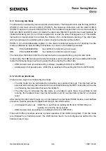
9.1.1 Entering Idle Mode
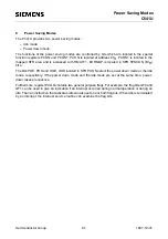
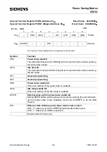
The idle mode is entered by two consecutive instructions. The first instruction sets the flag bit IDLE
(PCON.0) and must not set bit IDLS (PCON.5), the following instruction sets the start bit IDLS
(PCON.5) and must not set bit IDLE (PCON.0). The hardware ensures that a concurrent setting of
both bits, IDLE and IDLS, does not initiate the idle mode. Bits IDLE and IDLS will automatically be
cleared after being set. If one of these register bits is read the value that appears is 0. This double
instruction is implemented to minimize the chance of an unintentional entering of the idle mode
which would leave the watchdog timer’s task of system protection without effect.
PCON is not a bit-addressable register, so the above mentioned sequence for entering the idle
mode is obtained by byte-handling instructions,
as shown in the following example:
ORL
PCON,#00000001B
;Set bit IDLE, bit IDLS must not be set
ORL
PCON,#00100000B
;Set bit IDLS, bit IDLE must not be set
The instruction that sets bit IDLS is the last instruction executed before going into idle mode.
In idle mode, the USB module can be fully functional or can be switched off. If it is switched off in idle
mode the following steps must be processed before entering the idle mode :
– USB module clock is switched off by software (resetting bit UCLK in SFR DCR)
– additionally in full speed mode : USB PLL is switched off (resetting bit PCLK in SFR DCR)
9.1.2 Exit from Idle Mode
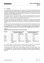
There are two ways to terminate the idle mode:
– The idle mode can be terminated by activating any enabled interrupt. This interrupt will be
serviced and normally the instruction to be executed following the RETI instruction will be the
one following the instruction that sets the bit IDLS.
– The other way to terminate the idle mode, is a hardware reset. Since the oscillator is still
running, the hardware reset must be held active only for two machine cycles for a complete
reset.
After leaving the idle mode through e.g. an interrupt with a switched-off USB module, a well defined
procedure must be executed foragain switching on the USB module :
– in full speed mode only
USB PLL is switched on (setting bit PCLK in SFR DCR) and
waiting 3 ms for PLL being locked
– USB module clock is switched on (setting bit UCLK in SFR DCR)
This switch off/on procedure assures a proper operation of the USB clock system. If the idle mode
is terminated by a hardware reset, the USB module has to be reconfigured as defined for the
hardware reset case.
Содержание C541U
Страница 1: ... 8 LW 026 0LFURFRQWUROOHU 8VHU V 0DQXDO http www siem ens d Sem iconductor ...
Страница 7: ......
Страница 21: ...Semiconductor Group 2 6 1997 10 01 Fundamental Structure C541U ...
Страница 37: ...Semiconductor Group 4 6 1997 10 01 External Bus Interface C541U ...
Страница 133: ...Semiconductor Group 6 88 1999 04 01 On Chip Peripheral Components C541U ...
Страница 163: ...Semiconductor Group 8 8 1997 10 01 Fail Safe Mechanisms C541U ...
Страница 185: ...Semiconductor Group 10 14 1997 10 01 OTP Memory Operation C541U ...
Страница 192: ...Semiconductor Group 12 7 Index C541U ...

