Semiconductor Group
10-12
1997-10-01
OTP Memory Operation
C541U
10.8
OTP Verify with Protection Level 1
If the C541U OTP program memory is protected in protection level 1), an OTP verification as shown
in figure 10-8 is used to verify the content of the OTP. The detailed timing characteristics of this
OTP verification mode is shown in the AC specifications (chapter 11).
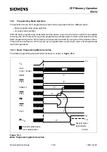
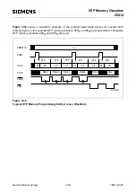
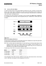
Figure 10-8
OTP Verification Mode Timing
The OTP verification mode is selected when the inputs PSEN, EA, and ALE are put to the specified
logic levels. With RESET going inactive, the OTP verification mode sequence is started. The C541U
outputs an ALE signal with a period of 3 CLPand expects data bytes at port 0. The data bytes at port
0 are assigned to the OTP addresses in the following way:
1. Data Byte =
content of internal OTP address 0000H
2. Data Byte =
content of internal OTP address 0001H
3. Data Byte =
content of internal OTP address 0002H
:
16. Data Byte =
content of internal OTP address 000FH
:
The C541U does not output any address information during the OTP verification mode. The first
data byte to be verified is always the byte which is assigned to the internal OTP address 0000H and
must be put onto the data bus with the first ALE pulse after the falling edge of RESET. With each
following ALE pulse the OTP address pointer is internally incremented and the expected data byte
for the next OTP address must be delivered externally.
Between two ALE pulses the data at port 0 is latched (at 3 CLP after ALE rising edge) and compared
internally with the OTP content of the actual address. If an verify error is detected, the error
RESET
ALE
Port 0
P3.5
6 CLP
3 CLP
Latch
Latch
Latch
Latch
Data for Addr. 0
Data for Addr. X 16
Data for Addr.
X 16 + 1
Data for Ad.
X 16 - 1
Data for
Addr. 1
Inputs : ALE =
PSEN, EA =
RESET =
V
SS
V
IH
MCT03289
1. ALE pulse
after reset
Low: Verify Error High: Verify ok
Содержание C541U
Страница 1: ... 8 LW 026 0LFURFRQWUROOHU 8VHU V 0DQXDO http www siem ens d Sem iconductor ...
Страница 7: ......
Страница 21: ...Semiconductor Group 2 6 1997 10 01 Fundamental Structure C541U ...
Страница 37: ...Semiconductor Group 4 6 1997 10 01 External Bus Interface C541U ...
Страница 133: ...Semiconductor Group 6 88 1999 04 01 On Chip Peripheral Components C541U ...
Страница 163: ...Semiconductor Group 8 8 1997 10 01 Fail Safe Mechanisms C541U ...
Страница 185: ...Semiconductor Group 10 14 1997 10 01 OTP Memory Operation C541U ...
Страница 192: ...Semiconductor Group 12 7 Index C541U ...


