Semiconductor Group
6-61
1999-04-01
On-Chip Peripheral Components
C541U
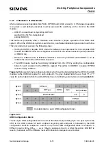
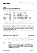
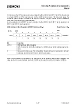
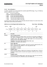
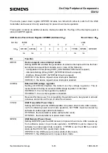
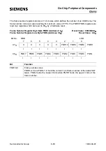
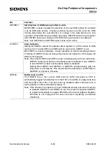
The device power down register DPWDR includes two bits which allow to switch off the USB
transmitter and receiver circuitry selectively for power down mode operation.
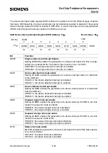
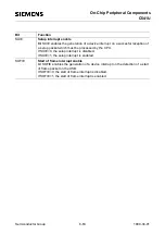
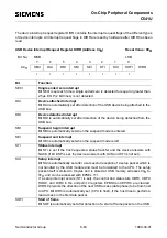
This register contains an additional device interrupt enable bit. The flag of the interrupt request is
stored in GEPIR register.
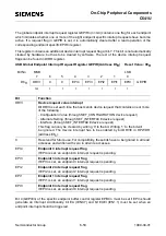
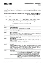
USB Device Power Down Register DPWDR (Address C2H) Reset Value : 00H
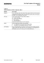
Bit
Function
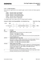
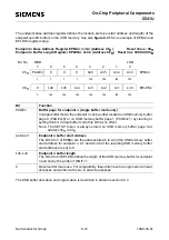
DRVIE
Device request value interrupt enable
Setting bit DRVIE enables the generation of a device interrupt each time the host
sends device request that contains one or more of the following :
- Configuration Value (through SET_CONFIGURATION device request)
- Alternate Setting (through SET_INTERFACE device request)
- Interface (through SET_INTERFACE device request)
If DRVIE=0, the device request value interrupt is disabled.
If DRVIE=1, the device request value interrupt is enabled.
XVREG
External USB voltage regulator
Setting bit XVREG disables the default on-chip voltage regulator. This is
recommended if using an external USB voltage regulator is intended.
If XVREG=0, the on-chip regulator is enabled.
If XVREG=1, the on-chip regulator is disabled.
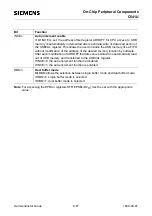
0
Reserved for future use. For compatiblity, these bits have to be ignored in all read
accesses and written with zero in all write accesses.
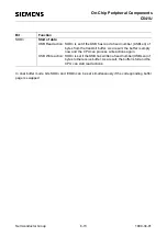
TPWD
USB Transmitter Power Down
Setting bit TPWD puts the USB transmitter into power down mode. After a wake-
up from software power down mode operation, bit TPWD must be cleared by
software to enable again data transmission.
If TPWD=0, the transmitter is active (default after reset).
If TPWD=1, the transmitter is in power down mode.
RPWD
USB Receiver Power Down
Setting bit RPWD puts the USB receiver into power down mode. After a wake-up
from software power down mode operation, bit RPWD must be cleared by
software to enable again data reception. If RPWD is set, the USB bus cannot
wake-up the C541U form power down mode.
If RPWD=0, the USB receiver is active (default after reset).
If RPWD=1, the USB receiver is in power down mode.
MSB
LSB
DPWDR
DRVIE XVREG
0
0
0
0
TPWD
RPWD
7
6
5
4
3
2
1
0
Bit No.
rw
rw
r
r
r
r
rw
rw
C2H
Содержание C541U
Страница 1: ... 8 LW 026 0LFURFRQWUROOHU 8VHU V 0DQXDO http www siem ens d Sem iconductor ...
Страница 7: ......
Страница 21: ...Semiconductor Group 2 6 1997 10 01 Fundamental Structure C541U ...
Страница 37: ...Semiconductor Group 4 6 1997 10 01 External Bus Interface C541U ...
Страница 133: ...Semiconductor Group 6 88 1999 04 01 On Chip Peripheral Components C541U ...
Страница 163: ...Semiconductor Group 8 8 1997 10 01 Fail Safe Mechanisms C541U ...
Страница 185: ...Semiconductor Group 10 14 1997 10 01 OTP Memory Operation C541U ...
Страница 192: ...Semiconductor Group 12 7 Index C541U ...

