Semiconductor Group
6-4
1999-04-01
On-Chip Peripheral Components
C541U
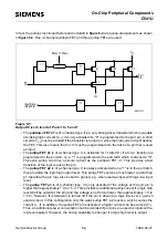
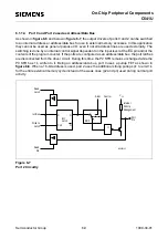
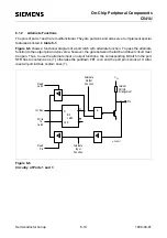
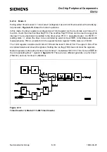
In fact, the pullups mentioned before and included in figure 6-2 are pullup arrangements as shown
in figure 6-3. One n-channel pulldown FET and three pullup FETs are used:
Figure 6-3
Output Driver Circuit of Ports 1 to 5 and 7
– The pulldown FET n1 is of n-channel type. It is a very strong driver transistor which is capable
of sinking high currents (
I
OL
); it is only activated if a "0" is programmed to the port pin. A short
circuit to
V
DD
must be avoided if the transistor is turned on, since the high current might destroy
the FET. This also means that no ”0“ must be programmed into the latch of a pin that is used
as input.
– The pullup FET p1 is of p-channel type. It is activated for 1 state (S1) if a 0-to-1 transition is
programmed to the port pin, i.e. a "1" is programmed to the port latch which contained a "0".
The extra pullup can drive a similar current as the pulldown FET n1. This provides a fast
transition of the logic levels at the pin.
– The pullup FET p2 is of p-channel type. It is always activated when a "1" is in the port latch,
thus providing the logic high output level. This pullup FET sources a much lower current than
p1; therefore the pin may also be tied to ground, e.g. when used as input with logic low input
level.
– The pullup FET p3 is of p-channel type. It is only activated if the voltage at the port pin is
higher than approximately 1.0 to 1.5 V. This provides an additional pullup current if a logic high
level shall be output at the pin (and the voltage is not forced lower than approximately 1.0 to
1.5 V). However, this transistor is turned off if the pin is driven to a logic low level, e.g when
used as input. In this configuration only the weak pullup FET p2 is active, which sources the
current
I
IL
. If, in addition, the pullup FET p3 is activated, a higher current can be sourced (
I
TL
).
Thus, an additional power consumption can be avoided if port pins are used as inputs with a
low level applied. However, the driving capability is stronger if a logic high level is output.
MCS03230
=1
1
=1
=1
V
CC
Port
Pin
SS
V
Q
Input Data
(Read Pin)
p1
p2
p3
n1
Delay = 1 State
_
<
Содержание C541U
Страница 1: ... 8 LW 026 0LFURFRQWUROOHU 8VHU V 0DQXDO http www siem ens d Sem iconductor ...
Страница 7: ......
Страница 21: ...Semiconductor Group 2 6 1997 10 01 Fundamental Structure C541U ...
Страница 37: ...Semiconductor Group 4 6 1997 10 01 External Bus Interface C541U ...
Страница 133: ...Semiconductor Group 6 88 1999 04 01 On Chip Peripheral Components C541U ...
Страница 163: ...Semiconductor Group 8 8 1997 10 01 Fail Safe Mechanisms C541U ...
Страница 185: ...Semiconductor Group 10 14 1997 10 01 OTP Memory Operation C541U ...
Страница 192: ...Semiconductor Group 12 7 Index C541U ...

