Semiconductor Group
6-50
1999-04-01
On-Chip Peripheral Components
C541U
6.4.4 USB Memory Buffer Address Generation
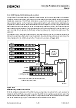
The generation of an USB memory address for USB access (read or write) depends on the EPNum
(endpoint number) information, which has been transmitted to the USB module during the software
initialization procedure. This EPNum information is used for the selection of an endpoint specific
base address register. As the maximum data packet length of each endpoint can individually be
programmed, there are some fixed start addresses for the endpoints. The user program defines the
base address for the first data byte of the corresponding endpoint by writing the endpoint specific
base address register EPBAn. The length depends on the amount of data to be read or written. The
user must take care to assign a buffer space at least as large as the maximum packet size of the
endpoint.
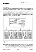
The address of the currently accessed byte in the USB memory area of the selected endpoint is
defined by an address offset, which must be added to the endpoint base address in order to get the
correct address for the USB memory buffer. The structure is shown in figure 6-32.
Figure 6-32
USB Memory Address Generation
With the software initialization of the USB module as described in section 6.4.5, each endpoint is
initialized with the EPNum value which is used at the USB memory address generation to select the
actual endpoint base address register. Further, in single buffer mode the bit PAGEn is used to select
one of the USB memory pages In dual buffer mode bit PAGEn has no effect.
MCD03411
PAGE 0
A06 A05 A04 A03
EPBA 0
A13
A14
A15
A16
PAGE 1
EPBA 1
A23
A24
A25
A26
PAGE 2
EPBA 2
A33
A34
A35
A36
PAGE 3
EPBA 3
A43
A44
A45
A46
PAGE 4
EPBA 4
MUX
of the actual
endpoint
EPNum
An4 An3
An5
An6
AO0
AO1
AO2
AO5
AO3
AO4
EPBAn
+ ADROFF
= USB Memory Addr.
AD4 AD3
AD5
AD6
AD2 AD1 AD0
An6 - An3
Page 1
Memory
Page 0
USB
Note: Only one bit of the bit pairs An5/AO5, An4/AO4,
An3/AO3 can be set at a time.
PAGEn
0
0
0
0
0
0
0
0
0
0
0
0
0
0
0
0
0
0
0
0
0
0
Содержание C541U
Страница 1: ... 8 LW 026 0LFURFRQWUROOHU 8VHU V 0DQXDO http www siem ens d Sem iconductor ...
Страница 7: ......
Страница 21: ...Semiconductor Group 2 6 1997 10 01 Fundamental Structure C541U ...
Страница 37: ...Semiconductor Group 4 6 1997 10 01 External Bus Interface C541U ...
Страница 133: ...Semiconductor Group 6 88 1999 04 01 On Chip Peripheral Components C541U ...
Страница 163: ...Semiconductor Group 8 8 1997 10 01 Fail Safe Mechanisms C541U ...
Страница 185: ...Semiconductor Group 10 14 1997 10 01 OTP Memory Operation C541U ...
Страница 192: ...Semiconductor Group 12 7 Index C541U ...


