Semiconductor Group
6-2
1999-04-01
On-Chip Peripheral Components
C541U
6.1.1 Port Structures
The C541U allows for digital I/O on 30 lines grouped into 4 bidirectional 8-/6-bit ports. Each port bit
consists of a latch, an output driver and an input buffer. Read and write accesses to the I/O ports P0
through P3 are performed via their corresponding special function registers P0 to P3.
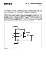
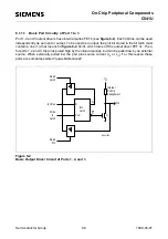
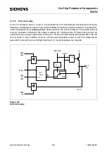
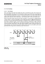
Figure 6-1 shows a functional diagram of a typical bit latch and I/O buffer, which is the core of each
of the 4 I/O-ports. The bit latch (one bit in the port’s SFR) is represented as a type-D flip-flop, which
will clock in a value from the internal bus in response to a "write-to-latch" signal from the CPU. The
Q output of the flip-flop is placed on the internal bus in response to a "read-latch" signal from the
CPU. The level of the port pin itself is placed on the internal bus in response to a "read-pin" signal
from the CPU. Some instructions that read from a port (i.e. from the corresponding port SFR P0 to
P3) activate the "read-latch" signal, while others activate the "read-pin" signal.
Figure 6-1
Basic Structure of a Port Circuitry
MCS01822
D
CLK
Port
Latch
Q
Q
Port
Read
Latch
to
Latch
Read
Pin
Write
Int. Bus
Port
Driver
Circuit
Pin
Содержание C541U
Страница 1: ... 8 LW 026 0LFURFRQWUROOHU 8VHU V 0DQXDO http www siem ens d Sem iconductor ...
Страница 7: ......
Страница 21: ...Semiconductor Group 2 6 1997 10 01 Fundamental Structure C541U ...
Страница 37: ...Semiconductor Group 4 6 1997 10 01 External Bus Interface C541U ...
Страница 133: ...Semiconductor Group 6 88 1999 04 01 On Chip Peripheral Components C541U ...
Страница 163: ...Semiconductor Group 8 8 1997 10 01 Fail Safe Mechanisms C541U ...
Страница 185: ...Semiconductor Group 10 14 1997 10 01 OTP Memory Operation C541U ...
Страница 192: ...Semiconductor Group 12 7 Index C541U ...

