Serial Peripheral Interface Controller
UG0331 User Guide Revision 15.0
509
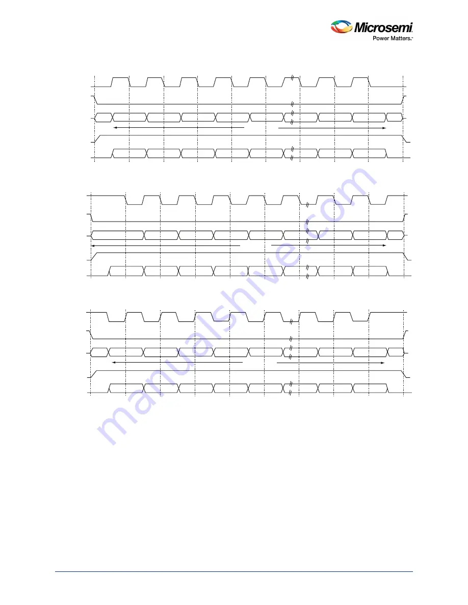
Single Frame Transfer – Mode 1: SPO = 0, SPH = 1
Figure 208 •
Motorola SPI Mode 1
Single Frame Transfer – Mode 2: SPO = 1, SPH = 0
Figure 209 •
Motorola SPI Mode 2
Single Frame Transfer – Mode 3: SPO = 1, SPH = 1
Figure 210 •
Motorola SPI Mode 3
14.2.2.3.2 Output Enable (SPI_X_DOE_N) Timing
Each SPI mode comprises two phases: transmit and receive. It is a requirement that the output enable
(SPI_X_DOE_N) line, which enables the output signal, should be driven so that the following occurs:
•
The output signal is ready to transmit when the data is available (setup time).
•
The output signal is held on long enough for the recipient to sample the data (hold time).
The minimum setup and hold time is one half SPI_X_CLK. In slave mode, the input clock is withdrawn at
the end of the transfer. For example, consider the waveform for Single Frame Transfer – Mode 2: SPO =
1, SPH = 0. In this case, data is sampled on the falling edge of the clock and shifted on the rising edge of
the clock. The data is sampled on the falling edge and must be held for one half SPI_X_CLK after the last
SPI_CLK
SPI_DI
SPI_DO
SPI_DOE_N
SPI_SS[x]
MSB
LSB
LSB
MSB
4 to 32 Bits
Q
Q
SPI_CLK
SPI_DI
SPI_DO
SPI_DOE_N
SPI_SS[x]
MSB
LSB
LSB
MSB
4 to 32 Bits
Q
SPI_CLK
SPI_DI
SPI_DO
SPI_DOE_N
SPI_SS[x]
MSB
LSB
LSB
MSB
4 to 32 Bits
Q
Q
Содержание SmartFusion2 MSS
Страница 1: ...UG0331 User Guide SmartFusion2 Microcontroller Subsystem ...
Страница 166: ...Cortex M3 Processor Reference Material UG0331 User Guide Revision 15 0 132 ...
Страница 200: ...Embedded NVM eNVM Controllers UG0331 User Guide Revision 15 0 166 Figure 87 System Builder Window ...
Страница 407: ...Universal Serial Bus OTG Controller UG0331 User Guide Revision 15 0 373 ...
Страница 806: ...Fabric Interface Controller UG0331 User Guide Revision 15 0 772 Figure 345 FIC Master AHB Lite Subsystem ...


