


UG-1262
Rev. B | Page 59 of 312
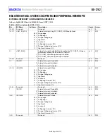
FFFF
C000
8000
16-
BI
T
A
DC
HE
X
CO
DE
4000
0000
0.2V
1.11V
2.02V
16
675
-00
8
Figure 9. Ideal ADC Transfer Function, Voltage Input to ADC vs. Output Codes, Where Input is ADCVBIAS_CAP at 1.11 V
To calculate the input voltage (V
IN
), use the following equation to convert ADC codes to a voltage:
For PGA gain = 1,
V
IN
= (
VREF
× (((
ADCDAT
− 0x8000)/2
15
)))
+ ADCVBIAS_CAP
(1)
For PGA gain = 1.5,
V
IN
= (
VREF
/1.5 × (((
ADCDAT
− 0x8000)/2
15
) × 1.835/1.82)) +
ADCVBIAS_CAP
For PGA gain = 2, 4, or 9,
V
IN
= (
VREF/PGA_GAIN
× (((
ADCDAT
− 0x8000)/2
15
)))
+ ADCVBIAS_CAP
where:
VREF
= 1.82 V (typical).
ADCDAT
is the ADC conversion result.
ADCVBIAS_CAP
= 1.11 V (typical).
PGA_GAIN
is the PGA gain setting minus one. This gain is set by ADCCON, Bits[18:16].
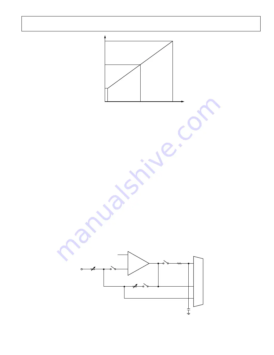
ADC LOW POWER CURRENT INPUT CHANNELS
Figure 10 shows the low power TIA0 input current channel, low power TIA0. The low power TIA1 input current channel, low power
TIA1, is identical to low power TIA0. The output of the low power TIA is the voltage proportional to the input current measured by the
ADC. Details on how to configure the R
LOAD0
resistor, R
TIA0
resistor, and low-pass filter programmable resistor (R
FILTER
) values can be
found in the Low Power TIAs section.
To select the low power TIA input channel for calibration and measurement, refer to ADCCON, Bits[12:0] in Table 63. For low power
TIA0, the ADC positive input is selected by setting ADCCON, Bits[5:0] = 0b000010. For low power TIA1, the ADC positive input is
selected by setting ADCCON, Bits[5:0] = 0b000011.
Figure 10 also shows the low power DAC (V
ZERO
) signal controlling the low power TIA positive input voltage level.
WE0
V
ZERO
R
TIA0
R
LOAD0
–
+
LOW
POWER
TIA0
R
FILTER
ADC
INPUT
MUX
LPF0
1667
5-
009
Figure 10. Low Power TIA0 Current Input Channel to the ADC


