


UG-1262
Rev. B | Page 100 of 312
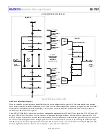
LPDAC1 SWITCH CONTROL REGISTER
Address: 0x400C2130, Reset: 0x00000000, Name: LPDACSW1
Table 117. Bit Descriptions for LPDACSW1
Bits Bit
Name Settings
Description
Reset
Access
[31:6] Reserved
Reserved.
0x0
R
5
LPMODEDIS
Switch Control. Controls switches connected to the output of LPDAC1.
0x0
R/W
0
Switches connected to output of low power DAC configured via LPDACCON1, Bit 5.
Default.
1
Overrides LPDACCON1, Bit 5. Switches connected to LPDAC1 output are controlled
via LPDACSW1, Bits[4:0].
4
SW4
LPDAC1 SW4 Control.
0x0
R/W
0
Disconnect direct connection of VBIAS0 DAC output to positive input of Low
Power Amplifier 1. Default.
1
Connect VBIAS1 DAC output directly to positive input of low power Amplifier 1.
3
SW3
LPDAC1 SW3 Control.
0x0
R/W
0
Disconnect VBIAS1 DAC output from low-pass filter and VBIAS1 pin.
1
Connect VBIAS1 DAC output to the low-pass filter and VBIAS1 pin. Default.
2
SW2
LPDAC1 SW2 Control.
R/W
0
Disconnect direct connection of VZERO0 DAC output to the low power TIA0 positive
input. Default.
0x0
1
Connect VZERO0 DAC output directly to the low power TIA0 positive input.
1
SW1
Low Power DAC1 SW1 Control.
0x0
R/W
0
Disconnect VZERO1 DAC output from the low-pass filter and VZERO1 pin.
1
Connect VZERO1 DAC output to the low-pass filter and VZERO1 pin. Default.
0
SW0
Low Power DAC1 SW0 Control.
0x0
R/W
0
Disconnect VZERO1 DAC output from the high speed TIA positive input. Default.
1
Connect VZERO1 DAC output to the high speed TIA positive input.
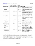
LPDAC1 CONTROL REGISTER
Address: 0x400C2134, Reset: 0x00000002, Name: LPDACCON1
Table 118. Bit Descriptions for LPDACCON1
Bits Bit
Name Settings
Description
Reset
Access
[31:7] Reserved
Reserved.
0x0
R
6
WAVETYPE
Low Power DAC Source.
0x0
R/W
0
Direct from LPDACDAT1.
1
Waveform
generator.
5 DACMDE
Low Power DAC1 Switch Settings. Control bit for the low power DAC1 output
switches.
0x0 R/W
0
Low Power DAC1 switches set for normal mode.
1
Low Power DAC1 switches set for diagnostic mode.
4 VZEROMUX
VZERO1 Output. Select which low power DAC1 output connects to the VZERO1
node. Ensure same value is written to the VBIASMUX bit. If this bit is set to 1,
LPDACCON1, Bit 3 = 1. If this bit is cleared to 0, LPDACCON1, Bit 3 = 0.
0x0 R/W
0
VZERO1 6-bit. Default. Clear to 0 for VZERO1 output to be 6-bit.
1
VZERO1 12-bit. Set to 1 for VZERO1 output to be 12-bit.
3 VBIASMUX
Bit Select. Select which low power DAC1 output connects to the VBIAS1 node.
Ensure same value is written to the VZEROMUX bit. If this bit is set to 1,
LPDACCON1, Bit 4 = 1. If this bit is cleared to 0, LPDACCON1, Bit 4 = 0.
0x0 R/W
0
12-bit output. Default. 12-bit DAC connects to the VBIAS1 pin.
1
6-bit output. 6-bit DAC connects to the VBIAS1 pin.
2
REFSEL
Low Power DAC1 Reference Select.
0x0
R/W
0
Select 2.5 V from low power buffer as DAC reference. Default.
1
Select AVDD power supply as DAC reference.