


UG-1262
Rev. B | Page 124 of 312
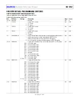
Px SWITCH MATRIX FULL CONFIGURATION REGISTER
Address: 0x400C2158, Reset: 0x00000000, Name: PSWFULLCON
This register allows individual control of the Px switches. The bit names are the same as the switch names shown in Figure 27.
SWCON, Bit 16 must be set to 1 after writing to this register for the new switch settings to take effect.
Table 147. Bit Descriptions for PSWFULLCON
Bits
Bit
Name Settings Description
Reset Access
[31:15] Reserved
Reserved.
0x0 R
14
PL2
Control of PL2 Switch. Control of PL2 switch.
0x0
R/W
0
Switch
open.
1
Switch
closed.
13
PL
Control of PL Switch. Shorts the D node and P node of the excitation amplifiers together.
0x0
R/W
0
Switch
open.
1
Switch
closed.
12 Reserved
Reserved.
0x0 R/W
11
P12
Control of P12 Switch. Connects the P node of the excitation amplifier to the CE1 pin.
0x0
R/W
0
Switch
open.
1
Switch
closed.
10
P11
Control of P11 Switch. Connects the P node of the excitation amplifier to the CE0 pin.
0x0
R/W
0
Switch
open.
1
Switch
closed.
9
P10
Control of P10 Switch. Connects the P node of the excitation amplifier to the DE1 pin.
0x0
R/W
0
Switch
open.
1
Switch
closed.
8
P9
Control of P9 Switch. Connects the P node of the excitation amplifier to the SE1 pin.
0x0
R/W
0
Switch
open.
1
Switch
closed.
7
P8
Control of P8 Switch. Connects the P node of the excitation amplifier to the DE0 pin.
0x0
R/W
0
Switch
open.
1
Switch
closed.
6
P7
Control of P7 Switch. Connects the P node of the excitation amplifier to the SE0 pin.
0x0
R/W
0
Switch
open.
1
Switch
closed.
5
P6
Control of P6 Switch. Connects the P node of the excitation amplifier to the RE1 pin.
0x0
R/W
0
Switch
open.
1
Switch
closed.
4
P5
Control of P5 Switch. Connects the P node of the excitation amplifier to the RE0 pin.
0x0
R/W
0
Switch
open.
1
Switch
closed.
3 P4
Control of P4 Switch. Connects the P node of the excitation amplifier to the
AIN3/BUF_VREF1V8 pin.
0x0 R/W
0
Switch
open.
1
Switch
closed.
2
P3
Control of P3 Switch. Connects the P node of the excitation amplifier to the AIN2 pin.
0x0
R/W
0
Switch
open.
1
Switch
closed.
1
P2
Control of P2 Switch. Connects the P node of the excitation amplifier to the AIN1 pin.
0x0
R/W
0
Switch
open.
1
Switch
closed.
0
PR0
Control of PR0 Switch. Connects the P node of the excitation amplifier to the RCAL0 pin.
0x0
R/W
0
Switch
open.
1
Switch
closed.


