


UG-1262
Rev. B | Page 132 of 312
POR
BOOT
INITIALIZATION
MEASUREMENT
HIBERNATE
HIBERNATE MODE WITH
SRAM CONTENTS
RETAINED
LOAD SEQUENCES TO SRAM,
SETUP SEQUENCE, FIFO, SLEEP AND
WAKE-UP TIMER, AND GPIOs.
RUN SEQUENCE
ENABLE/DISABLE
ANALOG BLOCKS,
START ADC CONVERSION,
STORE RESULTS IN SRAM
LOAD TRIM VALUES
MEASUREMENT
HIBERNATE
• • •
16
675
-331
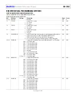
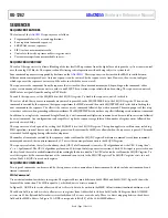
Figure 31. Run Sequence
Command Memory
The command memory stores the sequence commands and provides a link between the external microcontroller and the sequencer. The
command memory can be configured to use the 2 kB, 4 kB, and 6 kB SRAM memory sizes, which are selected using the CMDDATACON
register, Bits[2:0].
The large amount of memory available for the command memory facilitates the creation of larger, more complex sequences.
Determine the number of commands in a sequence by reading the SEQxINFO register, Bits[26:16].
The command memory is unidirectional. The host microcontroller specifies the destination address of the command by writing to the
CMDFIFOWADDR register and writes the command contents to the CMDFIFOWRITE register. The sequencer reads the commands from
memory for execution.
There are a number of interrupts associated with the command FIFO, including the FIFO threshold interrupt, the FIFO empty interrupt,
and the FIFO full interrupt. Refer to the AFE Interrupts section for more information.
Loading Sequences
The sequence commands are written to the SRAM by writing to two registers. The address in SRAM for the command is written to the
CMDFIFOWADDR register. The command content is written to the CMDFIFOWRITE register. When all commands are written to the
SRAM, write to the SEQxINFO registers to set the SEQ0 to SEQ3 information sequences.
Each information sequence from SEQ0 to SEQ3 requires a start address in SRAM and a total number of commands for that sequence.
The number of commands is written to the SEQxINFO register, Bits[26:16]. The start address is written to the SEQxINFO register,
Bits[10:0]. Ensure that there is no overlap between the four sequences. There is no hardware mechanism in place to warn the user of
overlapping sequences.
The interrupt sources associated with the sequencer include the following:
Sequence timeout error.
Sequencer timeout command finished.
End of sequence interrupt. For this interrupt to be asserted, the SEQCON register, Bit 0, must be cleared at the end of the sequencer
command.
Data FIFO
The data FIFO provides a buffer for the output of the analog and DSP blocks before the FIFO is read by the external controller.
The memory available for the data FIFO can be selected in the DATA_MEM_SEL bits in the CMDDATACON register. The available
memory options are 2 kB, 4 kB, and 6 kB. The data FIFO and command memory share the same block of 6 kB SRAM. Therefore, ensure
that there is no overlap between the command memory and the data FIFO.
The data FIFO can be configured in FIFO mode or stream mode via the CMDDATACON register, Bits[11:9]. In stream mode, when the FIFO
is full, old data is discarded to make room for new data. In FIFO mode, when the FIFO is full, new data is discarded. Do not let the FIFO
overflow when in FIFO mode. If there is overflow, all new data are lost.
The data FIFO is always unidirectional. A selectable source in the AFE block writes data and the external microcontroller reads data from
the DATAFIFORD register (see Table 220).
Select the data source for the data FIFO in the FIFOCON register, Bits[15:13] (see Table 219). The available source options include ADC
data, DFT result, sinc2 filter result, and statistic block mean result.


