


UG-1262
Rev. B | Page 133 of 312
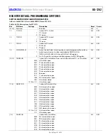
The interrupt flags associated with the data FIFO include empty, full, overflow, underflow, and threshold. These interrupts are user
readable using the INTCFLAGx registers (see the AFE Interrupts section for more details). Each flag has an associated maskable interrupt.
The overflow and underflow flags only activate for one clock period.
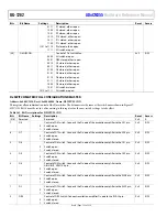
The data FIFO is enabled by writing a 1 to the FIFOCON register, Bit 11. The data FIFO threshold value is set by writing to the
DATAFIFOTHRES register. At any time, the host microcontroller can read the number of words in the data FIFO by reading the
FIFOCNTSTA register, Bits[26:16].
Reading data from the data FIFO when the FIFO is empty returns 0x00000000. The underflow flag, the FLAG27 bit, in the INTCFLAGx
register is also asserted.
Data FIFO Word Format
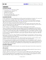
The format of data FIFO words is shown in Figure 32. Each word in the data FIFO is 32 bits. The seven MSBs are the ECC required for
functional safety applications. Bits[24:23] of the data FIFO word form the sequence identification (ID) and indicate which sequence, from
SEQ0 to SEQ3, the result came from.
Bits[22:16] of the data FIFO word contain the channel ID and indicate the source for the data (see Table 153).
The 16 LSBs of the data FIFO word are the actual data (see Figure 32).
When the data source is the DFT result, the data is 18 bits wide and is in twos complement format. The format is shown in Figure 33. The
channel ID is five bits wide, with 5'b11111 indicating the DFT results.
Sequencer and the Sleep and Wake-Up Timer
See the Sleep and Wake-Up Timer section for more information.
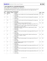
Sequencer Conflicts
If a conflict between sequences arises, for example, when SEQ0 is running and the SEQ1 request arrives, SEQ1 is ignored and SEQ0
completes. An interrupt is generated to indicate that the Sequence 1 is ignored.
Reading back registers does not cause resource conflicts. Writes to the MMRs by the processor are not allowed when the sequencer is
enabled. If conflicts arise, the sequencer has the priority. If the sequencer and the processor write at the same time, the host controller is
ignored. There is no error report for this conflict. Do not write to a register when the sequencer is running. However, there are registers
that are exceptions and can be written to freely without any conflict. The SEQCON register allows ending a sequence execution (SEQEN
bit) and halting a sequence (SEQHALT bit).
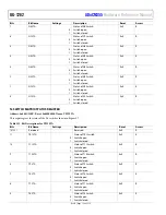
Table 153. Channel ID Description
Data FIFO Word, Bits[22:16]
Description
11111XX
1
DFT
result
11110XX
Mean from statistics block
1XXXXXX
Sinc2 filter result, XXXXXX is the ADC multiplexer positive setting (ADCCON Register, Bits[5:0])
0XXXXXX
Sinc3 filter result, XXXXXX is the ADC multiplexer positive setting (ADCCON Register, Bits[5:0])
1
X means don’t care.
[31:25]
[24:23]
[22:16]
[15:0]
7-BIT
ECC
2-BIT
SEQUENCE
ID
CHANNEL ID
16-BIT
DATA
16
67
5-
33
2
Figure 32. Data FIFO Word Format
[31:25]
[24:23]
[22:18]
[17:0]
7-BIT
ECC
2-BIT
SEQUENCE
ID
CHANNEL ID
5'b11111
18-BIT
DATA
16
67
5-
33
3
Figure 33. Data FIFO DFT Word Format


