


UG-1262
Rev. B | Page 104 of 312
USING DE0 AND DE1 INPUTS WITH THE HIGH SPEED TIA
To use DE0 as the input of the high speed TIA, set the following register values:
DE0RESCON = value required to set R
LOAD03
and R
TIA2_03
HSRTIACON, Bits[3:0] = 0xF to disconnect R
TIA2
from the high speed TIA.
DE1RESCON = 0xFF, to disconnect R
TIA2_05
from the high speed TIA.
To use DE1 as the output of the high speed TIA, set the following register values:
DE1RESCON = value required to set R
LOAD05
and R
TIA2_05
HSRTIACON, Bits[3:0] = 0xF to disconnect R
TIA2
from the high speed TIA.
DE1RESCON = 0xFF to disconnect R
TIA2_03
from the high speed TIA.
High Speed TIA Current Limit Feature
As well as the protection diode, the high speed TIA also has a built in current limiting feature. If the current sourced or sunk from the
TIA is greater than the overcurrent limit protection, the amplifier clamps the current to this limit. The current clamp typically clamps at
approximately 17 mA. Refer to the
data sheet for full specifications. Do not use this feature more frequently or for longer
than specified in the data sheet.
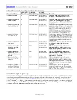
EXTERNAL R
TIA
SELECTION
The high speed TIA has the option of selecting an R
TIA
instead of the internal R
TIA2
, R
TIA2_03
, or R
TIA2_05
gain options. The DE0 pin
or DE1 pin can be connected to one side of the R
TIA
. This R
TIA
can be connected to the output of high speed TIA. The AIN0, AIN1, AIN2,
or AIN3/BUF_VREF1V8 pin can be connected to the other side of the external gain resistor, as shown in Figure 22.
To use the DE0 and AIN0 (input) pins to connect the high speed TIA with an R
TIA
, set the following register values:
DE0RESCON = 0x97 for 0 Ω R
LOAD03
and 0 Ω R
TIA2_03
in series with an external R
TIA
.
DE1RESCON = 0xFF.
HSRTIACON, Bits[3:0] = 0xF.
Close the T1 and T10 switches (configure the TSWFULLCON register).
HSTIA
HPTIA_N
R
TIA2_03
T10
EXTERNAL
R
TIA
HPTIA_P
1.11V REFERENCE
R
LOAD03
T1
DE0
AIN0
16
67
5-
12
5
Figure 22. Connecting External R
TIA
Across the High Speed TIA


