


UG-1262
Rev. B | Page 227 of 312
10-Bit Addressing
This feature is enabled by setting SCTL, Bit 1 for master and slave mode. The 10-bit address of the slave is stored in the ID0 register and
ID1 register, where the ID0 register contains the first byte of the address, and the R/W bit and the upper five bits must be programmed to
11110, as shown in Figure 58. The ID1 register contains the remaining eight bits of the 10-bit address. The ID2 register and ID3 register
can still be programmed with 7-bit addresses.
The master communicates to a 10-bit address slave using the ADR1 register and ADR2 registers. The format is described in Figure 58. To
perform a read from a slave with a 10-bit address, the master must first send a 10-bit address with the R/W bit cleared. It must then
generate a repeated start and send only the first byte of the address with the R/W bit set. A repeated start is generated by writing to the
ADR1 register while the master is still busy.
7
6
5
4
3
2
1
0
7
6
5
4
3
2
1
0
1
1
1
1
0
2 MSB
ADR1 AND ID0
ADR2 AND ID1
R/W
8 LSB
1667
5-
041
Figure 58. 10-Bit Address Format
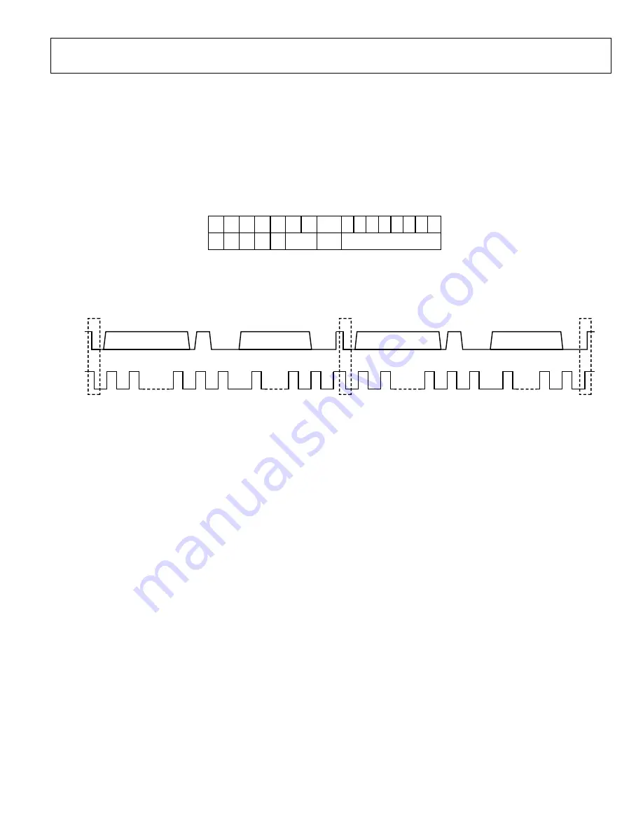
A repeated start condition occurs when a second start condition is sent to a slave without a stop condition being sent in between. This
sequence allows the master to reverse the direction of the transfer by changing the R/W bit without having to give up control of the bus.
An example of a transfer sequence is shown in Figure 59. This sequence is generally used in cases where the ability of the register to be
read is established by the first data sent to the device.
MSB
START
BIT
I2C_SCL
ACK
BIT
ACK
BIT
SLAVE ADDRESS
I2C_SDA
MSB
LSB
LSB
DATA
1
1
7
8
8
9
9
2
3 TO 6
2 TO 7
R/W
MSB
START
BIT
ACK
BIT
ACK
BIT
STOP
BIT
SLAVE ADDRESS
MSB
LSB
LSB
DATA
1
1
7
8
8
9
9
2
3 TO 6
2 TO 7
R/W
16
675
-042
Figure 59. I
2
C Repeated Start Sequence
On the slave side, an interrupt is generated (if enabled in the SCTL register) when a repeated start and a slave address are received. This
sequence is differentiated from receiving a start and slave address by using the start and REPSTART status bits in the SSTAT MMR.
On the master side, the master generates a repeated start if the ADR1 register is written while the master is still busy with a transaction.
After the I
2
C state machine has started to transmit the device address, it is safe to write to the ADR1 register.
For example, if a transaction involving a write, a repeated start, and then a read/write is required, write to the ADR1 register either after
the state machine starts to transmit the device address or after the first MTXREQ interrupt is received. When the transmit FIFO empties,
a repeated start is generated. Similarly, if a transaction involving a read, a repeated start, and then a read/write is required, write to the
first master address byte register, ADR1, either after the state machine starts to transmit the device address or after the first MRXREQ
interrupt is received. When the requested receive count is reached, a repeated start is generated.
I
2
C Clock Control
A PCLK clocks the I
2
C peripherals. CTL5, Bit 5 and CTL5, Bit 3 must be cleared to enable the clock to the I
2
C block. The frequency of
PCLK is determined by CTL1, Bits[13:8]. The I
2
C master in the system generates the serial clock for a transfer. The master channel can
be configured to operate in fast mode (400 kHz) or standard mode (100 kHz).
The bit rate is defined in the DIV MMR as follows:
f
SCL
=
f
I2CCLK
/(
Low
+
High
+ 3)
(21)
where:
f
SCL
is the I
2
C baud rate.
f
I2CCLK
is the PCLK frequency
.
Low
is the low period of the clock, DIV[7:0].
High
is the high period of the clock, DIV[15:8].
High = REQD_HIGH_TIME/PCLK_PERIOD
– 2
where:
REQD_HIGH_TIME
is the required high time period.
PCLK_PERIOD
is the PCLK period.


