


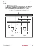


CCIX Transaction Layer
The Cache Coherent Interconnect for Accelerators (CCIX) transaction layer requirements are
implemented by the optional virtual channel 1 (VC1) in the design. Note that VC1 storage is in
addition to the PCI Express-compliant virtual channel 0 (VC0) storage. The CCIX transaction layer
interfaces with the CCIX protocol layer is implemented externally to the PCIe ports over the
CCIX transaction layer (ARM CXS) hard interface. For more information, see the Versal ACAP CPM
CCIX Architecture Manual (
).
Data Link Layer
The data link layer acts as an intermediate stage between the transaction layer and the physical
layer. Its primary responsibility is to provide a reliable mechanism for the exchange of information
between two components on a link. This includes data exchange (TLPs), error detection and
recovery, initialization services and the generation and consumption of data link layer packets
(DLLPs). DLLPs are used to transfer information between data link layers of two directly
connected components on the link. DLLPs convey information, such as power management, flow
control, and TLP acknowledgments. The data link layer supports 32 kilobyte replay buffers and
the feature DLLP.
Physical Layer
The physical layer interfaces the data link layer with signaling technology for link data
interchange, and is subdivided into the logical sub-block and the electrical sub-block.
• The logical sub-block frames and de-frames TLPs and DLLPs. It also implements the link
training and status state machine (LTSSM), which handles link initialization, training, and
maintenance. Scrambling and descrambling of data (for Gen1/Gen2/Gen3/Gen4 operation) is
also performed in this sub-block.
• The electrical sub-block defines the input and output buffer characteristics that interface the
device to the PCIe link. The physical layer also supports lane reversal (for multi-lane designs)
and lane polarity inversion, as required by the PCI Express Base Specification 4.0 (
).
Data exchange with the other components on the link occurs over the serial lines of one or more
gigabit transceivers (GTs), which expose parallel interfaces at lower clock frequencies to the PCIe
controller. For Gen1, Gen2, Gen3 and Gen4 operation, the physical layer is up-configuration
capable in the downstream port mode only.
Standards
The CPM4 block adheres to the following standards:
• PCI Express Base Specification 4.0 Version 1.0, and Errata updates (available at
Chapter 1: Overview
PG346 (v3.3) November 16, 2022
CPM Mode for PCI Express
8


