


Theory of Operation—2445 Service
Q709, Q741. U860A.. U910B, U980A, and associated
components.
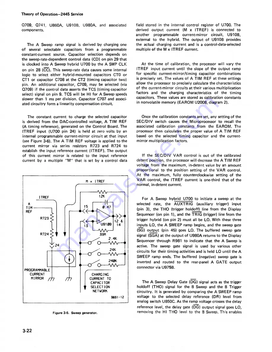
The A Sweep ramp signal is derived by charging one
o f several selectable capacitors from a programmable
constant-current source. Capacitor selection depends on
the sweep-rate-dependent control data (CD) on pin 29 that
is clocked into A Sweep hybrid U700 by the A SWP CLK
on pin 28 (CC). This sweep-rate data causes some internal
logic to select either hybrid-mounted capacitors CTO or
CT1 or capacitor C708 at the CT2 (timing capacitor two)
pin. An additional capacitor, C709, may be selected (via
Q709) if the control data asserts the TCS (timing capacitor
select) signal on pin 9. TCS w ill be HI for A Sweep speeds
slower than 1 ms per division. Capacitor C707 and associ
ated circuitry form a linearity compensation circuit.
The constant current to charge the selected capacitor
is derived from the DAC-controlled voltage, A TIM REF
(A tim ing reference), generated on the Control Board. The
ITREF input (U700 pin 24) is held at zero volts by an
internal programmable current-mirror circuit at that input
(see Figure 3-6). The A TIM REF voltage is applied to the
current m irror via series resistors R723 and R724 to
establish the input reference current (ITREF). The output
of this current m irror is related to the input reference
current by a multiple " M " that is set by a control data
field stored in the internal control register of U700. The
derived output current (M x ITREF) is connected to
another programmable current-mirror circuit, U910B,
external to the hybrid. The output o f U910B provides
the actual charging current and is a control-data-selected
multiple of the M x ITREF current.
A t the time of calibration, the processor w ill vary the
ITREF input current until the slope o f the output ramp
fo r specific current-mirror/timing capacitor combinations
is precisely set. The values of A TIM REF at these settings
allow the processor to precisely calculate the characteristics
o f the current-mirror circuits at their various m ultiplication
factors and the charging characteristics o f the timing
capacitors. These values are stored as calibration constants
in nonvolatile memory (EAROM U2008, diagram 2).
Once the calibration constants are set, any setting of the
SEC/DIV switch causes the Microprocessor to recall the
associated calibration constants from the EAROM. The
processor then calculates the proper value of A TIM REF
based on the selected tim ing capacitor and the current-
m irror m ultiplication factors.
If the SEC/DIV VAR control is out of the calibrated
detent position, the processor w ill decrease the A TIM REF
voltage from the maximum, in-detent value by an amount
proportional to the position setting of the VAR control.
A t the maximum, fu lly counterclockwise setting of the
VAR control, the ITREF current is one-third that of the
normal, in-detent current.
For A Sweep hybrid U700 to initiate a sweep at the
selected rate, the AUXTRIG (auxiliary trigger) input
(pin 3), the THO (trigger holdoff) line from the Display
Sequencer (on pin 1), and the TRIG (trigger) line from the
trigger hybrid (on pin 2) must all be LO. With these three
inputs LO, the A SWEEP ramp begins, and the sweep gate
(SG) output (pin 45) goes LO. The buffered sweep gate
signal (SGA) at the output of U980A returns to the Display
Sequencer through R981 to indicate that the A Sweep is
active. The sweep gate signal is used by various other
circuits fo r their tim ing activities and is held LO until the A
SWEEP ramp ends. The buffered (negative) sweep gate is
inverted and routed to the rear-panel A GATE output
connector via U975B.
The A Sweep Delay Gate (DG) signal acts as the trigger
holdoff (THO) signal for the B Sweep and the B Trigger
circuitry. It is generated by comparing the A SWEEP ramp
voltage to the selected delay reference (DR) level from
analog switch U850C. As the ramp voltage crosses the delay
reference level, the delay gate (DG) output signal goes LO,
removing the HI THO level to the B Sweep. This enables
3 - 2 2
Summary of Contents for 2445
Page 1: ...Tektronix 2445 OSCILLOSCOPE SERVICE INSTRUCTION MANUAL ...
Page 11: ...2445 Service 3829 01 The 2445 Oscilloscope ...
Page 44: ...Theory of Operation 2445 Service 3831 10A Figure 3 1 Block diagram ...
Page 45: ...Theory of Operation 2445 Service 3831 10B Figure 3 1 Block diagram cont 3 3 ...
Page 210: ...3829 58 Figure 9 4 2445 block diagram ...
Page 214: ......
Page 217: ......
Page 219: ...2445 382 72 ...
Page 222: ...2445 ...
Page 231: ...A 1 t C t t F t G t H t ...
Page 233: ......
Page 236: ......
Page 238: ...2445 392 1 75 ...
Page 244: ......
Page 247: ...A 1 C _____ D E F G H J 2445 3811 74 ...
Page 248: ...1 2 3 4 5 6 7 8 9 i o 2445 DISPLAY SEQUENCER TRIG GERING A4B SWEEPS ...
Page 253: ......
Page 263: ... 0 2445 J8 i S ...
Page 264: ...1 2 3 4 5 6 7 i 8 I i 9 10 2445 READOUT ...
Page 275: ......
Page 278: ......
Page 281: ......
Page 283: ... 8VJNR EG 3S 5 fROM P232 5 10 A 15VUNREG 8S F R O Mn i 2445 3 0 2 S 8 I ...
Page 286: ...2445 3823 82 ...
Page 290: ...B H le w o q 87V T S o I R v n i U1 R1873 PARTIAL A9 HIGH VOLTAGE BOARD 2445 ...
Page 299: ...2445 Service DAC REF A5 CONTROL ADJUSTMENT LOCATIONS 3 ...
Page 300: ......
Page 304: ...2 R E TU R N T O 1 ...
Page 305: ...ERROR MESSAGE DIAGNOSTICS ...
Page 306: ...ERROR MESSAGE DIAGNOSTICS ...
Page 307: ...O A A C t rnra g i tiw c t 3829 89 ...
Page 308: ...RETURN TO ...
Page 309: ...FRONT PANEL TROUBLESHOOTING ...
Page 310: ...FRONT PANEL TROUBLESHOOTING ...
Page 311: ...2445 Service 3829 90 ...
Page 316: ...R E TU R N T O v 1 y ...
Page 317: ...SWEEP TROUBLESHOOTING PROCEDURE ...
Page 323: ......
Page 324: ...2445 Service 3829 85 ...
Page 325: ......
Page 326: ... KERNEL NOP DIAGNOSTIC PROCEDURE ...
Page 327: ...10 POWER SUPPLY TROUBLESHOOTING PROCEDURE 3829 94 ...
Page 330: ......
Page 334: ...2445 Service REGULATOR TROUBLESHOOTING PROCEDURE 3829 93 ...
Page 338: ......
Page 346: ...12 2445 SERVICE ...
Page 347: ...2445 SERVICE ...
Page 348: ...2445 SERVICE ...


